Specific Process Knowledge/Etch/ICP Metal Etcher/silicon oxide: Difference between revisions
Appearance
No edit summary |
|||
| Line 1: | Line 1: | ||
'''Feedback to this page''': '''[mailto:labadviser@danchip.dtu.dk?Subject=Feed%20back%20from%20page%20http://labadviser.danchip.dtu.dk/index.php/Specific_Process_Knowledge/Etch/ICP_Metal_Etcher/silicon_oxide click here]''' | '''Feedback to this page''': '''[mailto:labadviser@danchip.dtu.dk?Subject=Feed%20back%20from%20page%20http://labadviser.danchip.dtu.dk/index.php/Specific_Process_Knowledge/Etch/ICP_Metal_Etcher/silicon_oxide click here]''' | ||
It is possible to etch SiO2 in the ICP metal etcher but it is not designed for it and the results are not fantastic. It is a challenge to get a good selectivity to resist (typically in the range of 1:1 or worse) and it is probably not possible to get a profile angle of 90 degrees. More likely about 75-85 degrees. | |||
===Slow etch of SiO2 with resist as masking material - using a 6" carrier wafer with recess === | ===Slow etch of SiO2 with resist as masking material - using a 6" carrier wafer with recess === | ||
Revision as of 11:55, 9 March 2015
Feedback to this page: click here
It is possible to etch SiO2 in the ICP metal etcher but it is not designed for it and the results are not fantastic. It is a challenge to get a good selectivity to resist (typically in the range of 1:1 or worse) and it is probably not possible to get a profile angle of 90 degrees. More likely about 75-85 degrees.
Slow etch of SiO2 with resist as masking material - using a 6" carrier wafer with recess
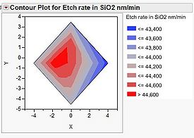
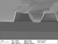
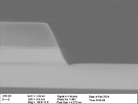
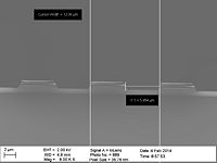
This recipe can be used for slow etching of SiO2 with resist as masking material. Here are some test results presented.
| Parameter | Resist mask |
|---|---|
| Coil Power [W] | 200 |
| Platen Power [W] | 25 |
| Platen temperature [oC] | 0 |
| CF4 flow [sccm] | 20 |
| H2 flow [sccm] | 10 |
| Pressure [mTorr] | 3 |


