Specific Process Knowledge/Thin film deposition/Furnace LPCVD PolySilicon: Difference between revisions
No edit summary |
|||
| Line 16: | Line 16: | ||
|- | |- | ||
!style="background:silver; color:black;" align="left"|Purpose | !style="background:silver; color:black;" align="left"|Purpose | ||
|style="background:LightGrey; color:black"|Deposition of silicon nitride | |style="background:LightGrey; color:black"|Deposition of silicon nitride | ||
|style="background:WhiteSmoke; color:black"|Stoichiometry: | |||
*Si<sub>3</sub>N<sub>4</sub> | *Si<sub>3</sub>N<sub>4</sub> | ||
*SRN | *SRN | ||
SRN: Silicon Rich Nitride | SRN: Silicon Rich Nitride | ||
|- | |- | ||
!style="background:silver; color:black" align="left"|Performance | !style="background:silver; color:black" align="left" valign="top" rowspan="3"|Performance | ||
|style="background:LightGrey; color:black"|Film thickness | |style="background:LightGrey; color:black"|Film thickness | ||
|style="background:WhiteSmoke; color:black"| | |||
*Si<sub>3</sub>N<sub>4</sub>:~50Å - ~3000Å | *Si<sub>3</sub>N<sub>4</sub>:~50Å - ~3000Å | ||
*SRN: ~50Å - ~10000Å | *SRN: ~50Å - ~10000Å | ||
|- | |- | ||
|style="background:LightGrey; color:black"|Step coverage | |||
|style="background:WhiteSmoke; color:black"| | |style="background:WhiteSmoke; color:black"| | ||
*Good | *Good | ||
|- | |- | ||
|style="background:LightGrey; color:black"|Film quality | |||
|style="background:WhiteSmoke; color:black"| | |style="background:WhiteSmoke; color:black"| | ||
*Dense film | *Dense film | ||
*Few defects | *Few defects | ||
|- | |- | ||
!style="background:silver; color:black" align="left"|Process parameter range | !style="background:silver; color:black" align="left" valign="top" rowspan="3"|Process parameter range | ||
|style="background:LightGrey; color:black"|Process Temperature | |style="background:LightGrey; color:black"|Process Temperature | ||
|style="background:WhiteSmoke; color:black"| | |style="background:WhiteSmoke; color:black"| | ||
*800-835 <sup>o</sup>C | *800-835 <sup>o</sup>C | ||
|- | |- | ||
|style="background:LightGrey; color:black"|Process pressure | |||
|style="background:WhiteSmoke; color:black"| | |style="background:WhiteSmoke; color:black"| | ||
*80-230 mTorr | *80-230 mTorr | ||
|- | |- | ||
|style="background:LightGrey; color:black"|Gas flows | |||
|style="background:WhiteSmoke; color:black"| | |style="background:WhiteSmoke; color:black"| | ||
*SiH<math>_2</math>Cl<math>_2</math>:10-100 sccm | *SiH<math>_2</math>Cl<math>_2</math>:10-100 sccm | ||
*NH<math>_3</math>:10-75 sccm | *NH<math>_3</math>:10-75 sccm | ||
|- | |- | ||
!style="background:silver; color:black" align="left"|Substrates | !style="background:silver; color:black" align="left" valign="top" rowspan="2"|Substrates | ||
|style="background:LightGrey; color:black"|Batch size | |style="background:LightGrey; color:black"|Batch size | ||
|style="background:WhiteSmoke; color:black"| | |style="background:WhiteSmoke; color:black"| | ||
| Line 55: | Line 57: | ||
*Deposition on both sides of the substrate | *Deposition on both sides of the substrate | ||
|- | |- | ||
| style="background:LightGrey; color:black"|Substrate material allowed | |||
|style="background:WhiteSmoke; color:black"| | |style="background:WhiteSmoke; color:black"| | ||
*Silicon wafers (new from the box or RCA cleaned) | *Silicon wafers (new from the box or RCA cleaned) | ||
Revision as of 16:02, 7 May 2008
Ikke skrevet!
LPCVD (Low Pressure Chemical Vapor Deposition) PolySilicon

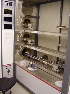
At the moment there is one furnace for PolySilicon depositions at Danchip. The furnace is a Tempress horizontal furnace. The process is a batch process meaning you can run a batch of 25 wafers at a time. The deposition takes place at temperatures of 800-835 degrees Celsius. The reactive gases are Ammonia and dichlorsilane. The LPCVD nitride has a good step coverage and the film thickness is very uniform over the wafer. We have two standard LPCVD nitride processes: One for depositing stoichiometric nitride (Si3N4) and one for deposition of low stress nitride (SNR). To get information on how to operate the furnace please read the manual which is uploaded to LabManager.
Process Knowledge
Please take a look at the process side for deposition of Silicon Nitride using LPCVD:
Deposition of Silicon Nitride using LPCVD
| Purpose | Deposition of silicon nitride | Stoichiometry:
SRN: Silicon Rich Nitride |
|---|---|---|
| Performance | Film thickness |
|
| Step coverage |
| |
| Film quality |
| |
| Process parameter range | Process Temperature |
|
| Process pressure |
| |
| Gas flows |
| |
| Substrates | Batch size |
|
| Substrate material allowed |
|
