Specific Process Knowledge/Thermal Process/Oxidation: Difference between revisions
| Line 41: | Line 41: | ||
|-style="background:WhiteSmoke; color:black" | |-style="background:WhiteSmoke; color:black" | ||
!Generel description | !Generel description | ||
|Drive-in of boron deposited in the | |Drive-in of boron deposited in the same furnace or drive-in of ion implanted boron. Can also be used for dry and wet oxidation. | ||
|Oxidation of gate-oxide and other | |Oxidation of gate-oxide and other very clean oxides. | ||
|Drive-in of phosphorous deposited in the phosphorous pre-dep furnace(A4) or drive-in of ion implanted phosphorous. Can also be used for dry and wet oxidation. | |Drive-in of phosphorous deposited in the phosphorous pre-dep furnace (A4) or drive-in of ion implanted phosphorous. Can also be used for dry and wet oxidation. | ||
|Oxidation of 6" wafers. Oxidation of new wafer with out RCA cleaning. Oxidation of wafers from the LPCVD furnaces and | |Oxidation of 4" and 6" wafers. Oxidation of new wafer with out RCA cleaning. Oxidation of wafers from the LPCVD furnaces and PECVD2. | ||
|Oxidation of wafers from EVG-NIL, PECVD3 and wafers with aluminum. | |Oxidation of wafers from EVG-NIL, PECVD3 and wafers with aluminum. | ||
|Oxidation of very thick oxides, thickness higher than 4 µm. | |Oxidation of very thick oxides, thickness higher than 4 µm. | ||
|Oxidation of almost materials on silicon | |Oxidation of almost all materials on silicon wafers. | ||
|- | |- | ||
| Line 98: | Line 98: | ||
|- | |- | ||
|-style="background:LightGrey; color:black" | |-style="background:LightGrey; color:black" | ||
!Process | !Process temperature | ||
| | | | ||
*900 <sup>o</sup>C - 1150 <sup>o</sup>C | *900 <sup>o</sup>C - 1150 <sup>o</sup>C | ||
| Line 136: | Line 136: | ||
Including one test wafer | Including one test wafer | ||
| | | | ||
*1-30 50 mm wafers | *1-30 50 mm wafers | ||
*1-30 100 mm wafers | *1-30 100 mm wafers | ||
Revision as of 16:57, 19 March 2014
Feedback to this page: click here
Oxidation
At Danchip we have seven furnaces for oxidation: A1, A2, A3, C1, C3, D1 and Noble. Oxidation can take place either by a dry process or a wet process. The film quality of dry oxide is better than for wet oxide with regards to density and dielectric constant, however the oxidation rate is slow for dry oxide. If the film quality for the wet oxide is acceptable then the thickness and the time it takes to grow the oxide often decides if a dry or wet oxidation is chosen.
- Dry oxidation is used from 5 nm - 200 nm and can be grown in the furnaces: A1, A2, A3, C1, C3.
- Wet oxidation is used up to 4 µm and can be grown in the furnaces: A1, A3, Noble.
- Very thick oxide >4 µm can be grown in D1, it is still a wet oxidation.
The standard recipes, quality control limits and results for the Boron Drive-in + Predep furnace (A1) and the Phosphorus Drive-in furnace (A3) can be found here:
- Standard recipes, QC limits and results for the Boron Drive-in + Predep furnace (A1)
- Standard recipes, QC limits and results for the Phosphorus Drive-in furnace (A3)
Comparison of the seven oxidation furnaces
| Generel description | Drive-in of boron deposited in the same furnace or drive-in of ion implanted boron. Can also be used for dry and wet oxidation. | Oxidation of gate-oxide and other very clean oxides. | Drive-in of phosphorous deposited in the phosphorous pre-dep furnace (A4) or drive-in of ion implanted phosphorous. Can also be used for dry and wet oxidation. | Oxidation of 4" and 6" wafers. Oxidation of new wafer with out RCA cleaning. Oxidation of wafers from the LPCVD furnaces and PECVD2. | Oxidation of wafers from EVG-NIL, PECVD3 and wafers with aluminum. | Oxidation of very thick oxides, thickness higher than 4 µm. | Oxidation of almost all materials on silicon wafers. |
|---|---|---|---|---|---|---|---|
| Oxidation method |
|
|
|
|
|
|
|
| Annealing gas |
|
|
|
|
|
|
|
| Process temperature |
|
|
|
|
|
|
|
| Substrate and Batch size |
Including one test wafer |
Including one test wafer |
Including one test wafer |
Including one test wafer |
Including one test wafer |
|
|
| Allowed materials |
All wafers have to be RCA cleaned. Except for Boron pre-dep wafer from furnace A1. |
All wafers have to be RCA cleaned. |
All wafers have to be RCA cleaned. Except for Phosphorous pre-dep wafers from furnace A4. |
All processed wafers have to be RCA cleaned. Except for wafers from LPCVD furnace and PECVD1. |
All wafers have to be RCA cleaned. Except for wafers from EVG-NIL, PECVD3 and wafer for annealing of aluminum. |
Only new wafers |
Almost all meterials |
Oxidation curves
Generic calculator for wet/dry oxide thickness calculation
The following links give an approximate oxide time/thickness based on a general formula.
Wet Oxidation on <100>
The curves below are based on measurements in our specific furnaces and give more accurate results. We will still recommend to make minimum one test run if the thickness is very important.
- Wet oxidation
-
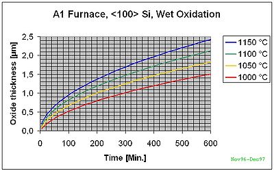 A1 Furnace <100>-Si Wet Oxidation
 -
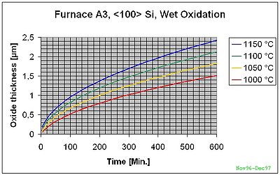 A3 Furnace <100>-Si Wet Oxidation


Dry Oxidation on <100> and <111> wafer
- Dry oxidation
-
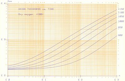 Dry oxide on <100> wafer. The y-axis is in Å and the x-axis is in minutes.
 -
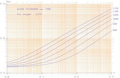 Dry oxide on <111> wafer. The y-axis is in Å and the x-axis is in minutes.

