Specific Process Knowledge/Etch/ICP Metal Etcher/silicon oxide: Difference between revisions
Appearance
No edit summary |
|||
| Line 34: | Line 34: | ||
!Results | !Results | ||
!Test on wafer with 50% load (Travka 50), by BGHE @danchip | !Test on wafer with 50% load (Travka 50), by BGHE @danchip | ||
!100% load on 100mm wafers with Barc and KRF (no mask) | |||
|- | |- | ||
|Etch rate of thermal oxide | |Etch rate of thermal oxide | ||
|'''44.1 nm/min (50% etch load) (01-02-2014)''' | |'''44.1 nm/min (50% etch load) (01-02-2014)''' | ||
| | |||
|- | |- | ||
|Selectivity to resist [:1] | |Selectivity to resist [:1] | ||
|'''~0.9''' | |'''~0.9''' (SiO2:resist) | ||
|'''~1.25:1 (Barc:KRF) | |||
|- | |- | ||
|Wafer uniformity (100mm) | |Wafer uniformity (100mm) | ||
|'''±1.6% (01-02-2014)''' | |'''±1.6% (01-02-2014)''' | ||
| | |||
|- | |- | ||
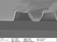
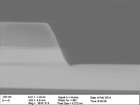
|Profile [<sup>o</sup>] | |Profile [<sup>o</sup>] | ||
|Take a look at the images but be aware that the resist profile was not good to begin with. | |Take a look at the images but be aware that the resist profile was not good to begin with. | ||
| | |||
|- | |- | ||
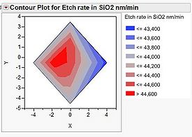
|Wafer uniformity map (click on the image to view a larger image) | |Wafer uniformity map (click on the image to view a larger image) | ||
|[[image:ICP_metal_slow_wafer_uniformity_s4075.jpg|275x275px|center|thumb|Contour plot of the etch rate over the wafer, 9 points measured]] | |[[image:ICP_metal_slow_wafer_uniformity_s4075.jpg|275x275px|center|thumb|Contour plot of the etch rate over the wafer, 9 points measured]] | ||
| | |||
|- | |- | ||
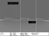
|SEM profile images | |SEM profile images | ||
| Line 57: | Line 63: | ||
image:ICP_metal_slow_s4075_sio2_6.jpg|Resist profiler after etch 01-02-2014. No line width reduction observed. | image:ICP_metal_slow_s4075_sio2_6.jpg|Resist profiler after etch 01-02-2014. No line width reduction observed. | ||
</gallery> | </gallery> | ||
| | |||
|- | |||
|Etch rate in barc | |||
| | |||
|50 nm/min (2014-09-09) | |||
|- | |||
|Etch rate in KRF resist | |||
|40 nm/min (2014-09-09) | |||
|- | |- | ||
|} | |} | ||
<br/> | <br/> | ||
Revision as of 11:03, 9 September 2014
Feedback to this page: click here
Slow etch of SiO2 with resist as masking material - using a 6" carrier wafer with recess
This recipe can be used for slow etching of SiO2 with resist as masking material. Here are some test results presented.
| Parameter | Resist mask |
|---|---|
| Coil Power [W] | 200 |
| Platen Power [W] | 25 |
| Platen temperature [oC] | 0 |
| CF4 flow [sccm] | 20 |
| H2 flow [sccm] | 10 |
| Pressure [mTorr] | 3 |


