Specific Process Knowledge/Etch/ICP Metal Etcher/silicon oxide: Difference between revisions
Appearance
| Line 44: | Line 44: | ||
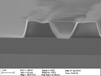
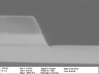
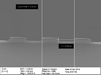
|Take a look at the images but be aware that the resist profile was not good to begin with. | |Take a look at the images but be aware that the resist profile was not good to begin with. | ||
|- | |- | ||
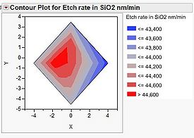
| | |Wafer uniformity map (click on the image to view a larger image) | ||
|[[image:ICP_metal_slow_wafer_uniformity_s4075.jpg|275x275px| | |[[image:ICP_metal_slow_wafer_uniformity_s4075.jpg|275x275px|center|thumb|Contour plot of the etch rate over the wafer, 9 points measured]] | ||
|- | |- | ||
|SEM profile images | |SEM profile images | ||
Revision as of 11:18, 17 February 2014
Slow etch of SiO2 with resist as masking material - with direct clamping 
This recipe can be used for slow etching of SiO2 with resist as masking material when normal clamping is possible. Normal clamping is prefered because it give the best and most repeatable cooling of the wafer. Here are some test results presented.
| Parameter | Resist mask |
|---|---|
| Coil Power [W] | 200 |
| Platen Power [W] | 25 |
| Platen temperature [oC] | 0 |
| CF4 flow [sccm] | 20 |
| H2 flow [sccm] | 10 |
| Pressure [mTorr] | 3 |


