Specific Process Knowledge/Characterization/SEM: Scanning Electron Microscopy: Difference between revisions
| Line 62: | Line 62: | ||
* Any sample except bulk insulators such as polymers, glass or quartz wafers | * Any sample except bulk insulators such as polymers, glass or quartz wafers | ||
|style="background:WhiteSmoke; color:black"| | |style="background:WhiteSmoke; color:black"| | ||
* Any sample except bulk insulators such as polymers, glass or quartz wafers | * Any sample except bulk insulators such as polymers, glass or quartz wafers | ||
|style="background:WhiteSmoke; color:black"| | |style="background:WhiteSmoke; color:black"| | ||
* All samples | * All samples | ||
Revision as of 13:36, 10 March 2014
Feedback to this page: click here


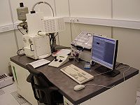
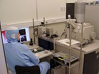
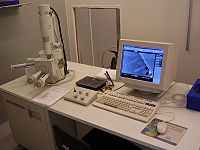
Scanning electron microscopy at Danchip
The SEM's at Danchip cover a wide range of needs both in the cleanroom and outside: From the fast in-process verification of different process parameters such as etch rates, step coverages or lift-off quality to the ultra high resolution images on any type of sample intended for publication.
The 'workhorse' SEM that will cover most users needs is the Leo SEM. It is a very reliable and rugged instrument that provides high quality images of most samples. Excellent images on a large variety of materials such as semiconductors, semiconductor oxides or nitrides, metals, thin films and some polymers may be acquired on the Leo SEM. As such, we prefer that new users that have no prior SEM experience get trained on the Leo SEM before they start using the other SEM's.
The Zeiss SEM and the Supra 60 VP SEM are both 'Supra VP' models from Carl Zeiss (a 40 and 60 respectively). As such they share a lot of similaritites but they also differ in some respects. The SmartSEM operator software installed on both these SEM's is also running on the Leo. This is very convenient as it allows the users to shift between instruments quite easily.
The Zeiss SEM was installed in the cleanroom in 2010 and quickly became the 'Weapon of choice' for many SEM users. It's a state-of-the-art SEM that will produce excellent images on any sample. The possibility of operating at higher chamber pressures in the VP mode makes imaging of bulk non-conducting samples possible.
The Supra 60 VP SEM is basically the same as the Zeiss SEM but with some additional features such as an airlock and an EDX detector.
The FEI SEM is a versatile microscope with two vacuum modes (High Vacuum and Low Vacuum) and 6 different detectors, offering excellent resolution on any type of sample or material including graphene and carbon nanotubes. Somewhat more fragile compared to the robust Leo, it is our intention that only users with special needs (for instance thick polymers, glass substrates or EDX/micromanipulator experiments) that will be trained.
Outside the cleanroom in the basement of building 346, the Jeol SEM provides a possibilty of imaging samples that do not go into the cleanroom.
The user manuals, quality control procedures and results, user APVs, technical information and contact information can be found in LabManager:
- The SEM Leo page in LabManager,
- The SEM FEI page in LabManager,
- The SEM Zeiss page in LabManager,
- The SEM Supra 60 VP page in LabManager,
- The SEM Jeol page in LabManager,
Process information
| Equipment | SEM Leo | SEM Zeiss | SEM Supra 60VP | SEM FEI | SEM Jeol | |
|---|---|---|---|---|---|---|
| Model | Leo 1550 SEM | Zeiss Supra 40 VP | Zeiss Supra 60 VP | FEI Nova 600 NanoSEM | Jeol JSM 5500 LV | |
| Purpose | Imaging and measurement of |
|
|
|
|
|
| Performance | Resolution | The resolution of a SEM is strongly dependent on the type of sample and the skills of the operator. The highest resolution is probably only achieved on special samples | ||||
|
|
|
|
| ||
| Instrument specifics | Detectors |
|
|
|
|
|
| Stage |
|
|
|
|
| |
| Electron source |
|
|
|
|
| |
| Operating pressures |
|
|
|
|
| |
| Substrates | Sample sizes |
|
|
|
|
|
| Allowed materials |
|
|
|
|
| |
