Specific Process Knowledge/Thin film deposition/PECVD: Difference between revisions
| Line 32: | Line 32: | ||
|style="background:LightGrey; color:black"|Deposition of dielectrica | |style="background:LightGrey; color:black"|Deposition of dielectrica | ||
|style="background:WhiteSmoke; color:black"| | |style="background:WhiteSmoke; color:black"| | ||
* | *Silicon oxide | ||
*Silicon nitride | |||
*Silicon oxynitride | |||
*PBSG (Phosphorous Boron doped Silica Glass) | |||
*Silicon oxide doped with Germanium | |||
| | | | ||
*Silicon oxide | *Silicon oxide | ||
| Line 43: | Line 47: | ||
|style="background:LightGrey; color:black"|Film thickness | |style="background:LightGrey; color:black"|Film thickness | ||
|style="background:WhiteSmoke; color:black"| | |style="background:WhiteSmoke; color:black"| | ||
* | *~10nm - 30µm | ||
| | | | ||
*~10nm - 30µm | *~10nm - 30µm | ||
| Line 49: | Line 53: | ||
|style="background:LightGrey; color:black"|Index of refraction | |style="background:LightGrey; color:black"|Index of refraction | ||
|style="background:WhiteSmoke; color:black"| | |style="background:WhiteSmoke; color:black"| | ||
* | *~1.4-2.1 | ||
| | | | ||
*~1.4-2.1 | *~1.4-2.1 | ||
| Line 55: | Line 59: | ||
|style="background:LightGrey; color:black"|Step coverage | |style="background:LightGrey; color:black"|Step coverage | ||
|style="background:WhiteSmoke; color:black"| | |style="background:WhiteSmoke; color:black"| | ||
* | *In general: Not so good | ||
*PBSG: Floats at 1000<sup>o</sup>C | |||
| | | | ||
*In general: Not so good | *In general: Not so good | ||
| Line 62: | Line 67: | ||
|style="background:LightGrey; color:black"|Film quality | |style="background:LightGrey; color:black"|Film quality | ||
|style="background:WhiteSmoke; color:black"| | |style="background:WhiteSmoke; color:black"| | ||
* | *Not so dense film | ||
*Hydrogen will be incorporated in the films | |||
| | | | ||
*Not so dense film | *Not so dense film | ||
| Line 70: | Line 76: | ||
|style="background:LightGrey; color:black"|Process Temperature | |style="background:LightGrey; color:black"|Process Temperature | ||
|style="background:WhiteSmoke; color:black"| | |style="background:WhiteSmoke; color:black"| | ||
* | *300 <sup>o</sup>C | ||
| | | | ||
*300 <sup>o</sup>C | *300 <sup>o</sup>C | ||
| Line 76: | Line 82: | ||
|style="background:LightGrey; color:black"|Process pressure | |style="background:LightGrey; color:black"|Process pressure | ||
|style="background:WhiteSmoke; color:black"| | |style="background:WhiteSmoke; color:black"| | ||
* | *~200-900 mTorr | ||
| | | | ||
*~200-900 mTorr | *~200-900 mTorr | ||
| Line 82: | Line 88: | ||
|style="background:LightGrey; color:black"|Gas flows | |style="background:LightGrey; color:black"|Gas flows | ||
|style="background:WhiteSmoke; color:black"| | |style="background:WhiteSmoke; color:black"| | ||
* | *SiH<math>_4</math>:0-60 sccm | ||
*N<math>_2</math>O:0-3000 sccm | |||
*NH<math>_3</math>:0-1000 sccm | |||
*N<math>_2</math>:0-3000 sccm | |||
*GeH<math>_4</math>:0-6.00 sccm | |||
*5%PH<math>_3</math>:0-99 sccm | |||
*5%B<math>_2</math>H<math>_6</math>:0-1000 sccm | |||
| | | | ||
*SiH<math>_4</math>:0-60 sccm | *SiH<math>_4</math>:0-60 sccm | ||
Revision as of 12:24, 27 January 2014
Feedback to this page: click here
PECVD Plasma Enhanced Chemical Vapor Deposition


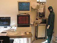
We have two (three) PECVD's here at DANCHIP. They can all be used to deposit Silicon oxides and Silicon nitrides with or without dopants of Boron, Phosphorus and Germanium. PECVD1 has been decommissioned and PECVD3 are used for silicon based processing with small amounts (<5% wafer coverage) of metals where as PECVD2 is dedicated for clean wafers both for silicon based materials and III-V materials. Quartz carriers are used in PECVD2 and they are dedicated the two different material groups to avoid cross contamination. See the precise rules in the equipment manuals which are uploaded in LabManager.
PECVD is a chemical vapor deposition process that applies a plasma to enhance chemical reaction rates of reactive spices. PECVD processing allows deposition at lower temperatures, which is often critical in the manufacture of semiconductors.
All though PECVD2 and 3 are very similar you should not expect to transfer a recipe between the systems and get the exact same result.
Recipes on PECVD1(will be removed soon), PECVD2 and PECVD3
- Recipes for PECVD2 are in the III-V entry in LAbAdviser, see here
- Recipes on PECVD1 for deposition of silicon oxides
- Recipes on PECVD1 for deposition of silicon nitride and silicon oxynitride
- Recipes on PECVD3 for deposition of silicon oxides
- Recipes on PECVD3 for deposition of silicon nitride and silicon oxynitride
| PECVD | PECVD2 | PECVD3 | |
|---|---|---|---|
| Purpose | Deposition of dielectrica |
|
|
| Performance | Film thickness |
|
|
| Index of refraction |
|
| |
| Step coverage |
|
| |
| Film quality |
|
| |
| Process parameter range | Process Temperature |
|
|
| Process pressure |
|
| |
| Gas flows |
|
| |
| Substrates | Batch size |
|
|
| Substrate material allowed |
|
| |
| Material allowed on the substrate |
|
| |
