Specific Process Knowledge/Characterization/Drop Shape Analyzer: Difference between revisions
Appearance
| Line 16: | Line 16: | ||
[http://labmanager.danchip.dtu.dk/function.php?module=Machine&view=view&mach=240 Drop Shape Analyzer in LabManager] | [http://labmanager.danchip.dtu.dk/function.php?module=Machine&view=view&mach=240 Drop Shape Analyzer in LabManager] | ||
== | ==An overview of the performance of the Prism Coupler== | ||
{| border="2" cellspacing="0" cellpadding="10" | |||
|- | |||
!style="background:silver; color:black;" align="left"|Purpose | |||
* | |style="background:LightGrey; color:black"|Film thickness measurements and optical characterization of optically transparent thin films||style="background:WhiteSmoke; color:black"| | ||
* | *Measurement of film thickness | ||
* | *Optical constants | ||
* | |- | ||
!style="background:silver; color:black" align="left"|Performance | |||
== | |style="background:LightGrey; color:black"|Thin film materials that can be measured||style="background:WhiteSmoke; color:black"| | ||
Film with a refractive index of less than 2.02 and that are transparent to the light in the given wavelength range | |||
ex: | |||
*Silicon Oxide | |||
*Silicon nitride | |||
*polymers | |||
|- | |||
|style="background:silver; color:black"| | |||
|style="background:LightGrey; color:black"|Film thickness range | |||
|style="background:WhiteSmoke; color:black"| | |||
*~1µm to 15 µm | |||
|- | |||
|style="background:silver; color:black"| | |||
|style="background:LightGrey; color:black"|Film thickness accuracy | |||
|style="background:WhiteSmoke; color:black"| | |||
*±(0.5%+50Å) | |||
|- | |||
|style="background:silver; color:black"| | |||
|style="background:LightGrey; color:black"|Index accuracy | |||
|style="background:WhiteSmoke; color:black"| | |||
*±0.001 | |||
|- | |||
!style="background:silver; color:black" align="left"|Process parameter range | |||
|style="background:LightGrey; color:black"|Wavelength range | |||
|style="background:WhiteSmoke; color:black"| | |||
Can operate at two different wavelength: | |||
*633 nm | |||
*1550 nm | |||
|- | |||
!style="background:silver; color:black" align="left"|Substrates | |||
|style="background:LightGrey; color:black"|Batch size | |||
|style="background:WhiteSmoke; color:black"| | |||
*One sample at a time - all sample larger than 5x5 mm<sup>2</sup>sizes up to 6" | |||
|- | |||
|style="background:silver; color:black"| | |||
| style="background:LightGrey; color:black"|Substrate material allowed | |||
|style="background:WhiteSmoke; color:black"| | |||
*In principle all materials | |||
|- | |||
|} | |||
Revision as of 13:28, 10 January 2014
Feedback to this page: click here
THIS PAGE IS UNDER CONSTRUCTION
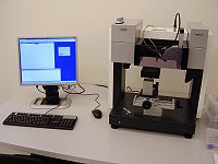
The Drop Shape Analyzer
The Krüss DSA 100S Drop Shape Analyzer will analyze the shapes of drops of liquid on a surface or suspended from a needle in order to calculate the contact angle or the surface tension, respectively.

The user manual, user APV(s), technical information, and contact information can be found in LabManager:
Drop Shape Analyzer in LabManager
An overview of the performance of the Prism Coupler
| Purpose | Film thickness measurements and optical characterization of optically transparent thin films |
|
|---|---|---|
| Performance | Thin film materials that can be measured |
Film with a refractive index of less than 2.02 and that are transparent to the light in the given wavelength range ex:
|
| Film thickness range |
| |
| Film thickness accuracy |
| |
| Index accuracy |
| |
| Process parameter range | Wavelength range |
Can operate at two different wavelength:
|
| Substrates | Batch size |
|
| Substrate material allowed |
|
