Specific Process Knowledge/Characterization/AFM: Atomic Force Microscopy: Difference between revisions
No edit summary |
No edit summary |
||
| Line 19: | Line 19: | ||
==Process Information== | ==Process Information== | ||
[[Image:Tap300Al-G.jpg|right|thumb|Std. tip Tap300Al-G]] | |||
[[Image:Tap300Al-G-schematic.png|right|thumb|Std. tip Tap300Al-G]] | |||
[[Image:SSS-NCHR-AFM-tip.jpg|right|thumb|SSS-NCHR tip<br /> (Super-Sharp-Silicon)]] | |||
[[Image:Nanoman cantilever AR5.jpg|right|thumb|AR5-NCHR tip<br /> (Aspect ratio 5)]] | |||
For a tutorial on AFM see here: [http://www.doitpoms.ac.uk/tlplib/afm/index.php AFM] | For a tutorial on AFM see here: [http://www.doitpoms.ac.uk/tlplib/afm/index.php AFM] | ||
Free analysis software: For visualizing and analyzing AFM and Optical profiler files (Nanoman and Sensofar) [http://gwyddion.net Gwyddion] | Free analysis software: For visualizing and analyzing AFM and Optical profiler files (Nanoman and Sensofar) [http://gwyddion.net Gwyddion] | ||
==An overview of the performance of the AFM: Nanoman== | ==An overview of the performance of the AFM: Nanoman== | ||
{| border="2" cellspacing="0" cellpadding="2" | {| border="2" cellspacing="0" cellpadding="2" | ||
Revision as of 12:06, 9 January 2014
Feedback to this page: click here
Nanoman
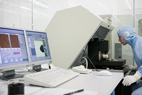
The AFM: Nanoman is a product of Bruker. AFM stands for Atomic Force Microscope which is a scanning probe microscope where a sharp probe is scanned across a surface either in contact mode or tapping mode. The outcome is a topographic plot of the surface. It has a lateral solution of about 1 nm and a vertical resolution of less than 1 Å which makes it very suitable for topographic characterization in the nanometer regime. The limiting factor however is often the size of the probe in use. The tip radius of curvature (ROC) can be from 2 nm up to more than 20 nm depending on the chosen probe. The half cone angle of the tip can vary from less than 3o to over 25o giving problems resolving high aspect ratio structures.
The main purposes are surface roughness measurements and step/structure high measurements in the nanometer and sub-micrometer regime. For larger structure see the topografic measurement page.
To get some product information from the vendor take a look at Bruker's homepage [1] (Bruker acquired Veeco's AFM business in Oct. 2010)
The user manual(s), quality control procedure(s) and results, user APV(s), technical information and contact information can be found in LabManager:
Nanoman in LabManager
Process Information
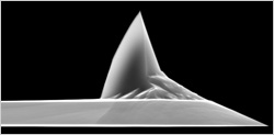
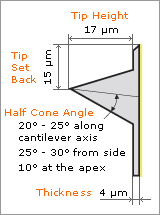
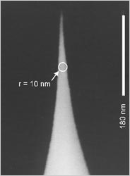
(Super-Sharp-Silicon)
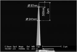
(Aspect ratio 5)
For a tutorial on AFM see here: AFM
Free analysis software: For visualizing and analyzing AFM and Optical profiler files (Nanoman and Sensofar) Gwyddion
An overview of the performance of the AFM: Nanoman
| Equipment | Nanoman | |
|---|---|---|
| Purpose | Topografic measurement in the nanometer and and sub-micrometer regime |
|
| Performance | Scan range xy | Up to 90 µm square |
| Scan range z | 1 µm (can go up to 6µm with special settings) | |
| Resolution xy | Down to 1.4 nm - accuracy better than 2% | |
| Resolution z | <1 Å - accuracy better than 2% | |
| Max. scan depth as a function of trench width W | ~1 for our standard probe. Can be improved to about 10 with the right probe | |
| Hardware settings | Tip radius of curvature | Standard probe: <12 nm |
| Standard Cantilevers/tips | Tap300Al-G | |
| Super Sharp Si Cantilever/tip | SSS-NCHR | |
| High Aspect Ratio Cantilever/tip | AR5-NCHR | |
| Cantilevers/tips vendor | www.nanoandmore.com | |
| Substrates | Substrate size | Up to 6" |
| Substrate material allowed | In principle all materials | |
