Specific Process Knowledge/Characterization/AFM: Atomic Force Microscopy: Difference between revisions
Appearance
| Line 3: | Line 3: | ||
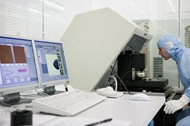
[[image:Nanoman.jpg|275x275px|right|thumb|Nanoman: positioned in cleanroom 4 - glass cage no. 4]] | [[image:Nanoman.jpg|275x275px|right|thumb|Nanoman: positioned in cleanroom 4 - glass cage no. 4]] | ||
The AFM: Nanoman is a product of Veeco Instruments. | The AFM: Nanoman is a product of Veeco Instruments. AFM stands for Atomic Force Microscope which is a scanning probe microscope where a sharp probe is scanned across a surface either in contact mode or tapping mode. The outcome is a topographic plot of the surface. It has a lateral solution at about 1 nm and a vertical resolution of less than 1 Å which makes it very suitable for topographic characterization in the nanometer regime. The limiting factor however is often the size of the probe in use. The | ||
To get some product information from the vendor take a look at Veeco's homepage [http://www.veeco.com/products/details.php?cat=1&sub=1&pid=178] | To get some product information from the vendor take a look at Veeco's homepage [http://www.veeco.com/products/details.php?cat=1&sub=1&pid=178] | ||
Revision as of 14:30, 8 January 2008
Nanoman

The AFM: Nanoman is a product of Veeco Instruments. AFM stands for Atomic Force Microscope which is a scanning probe microscope where a sharp probe is scanned across a surface either in contact mode or tapping mode. The outcome is a topographic plot of the surface. It has a lateral solution at about 1 nm and a vertical resolution of less than 1 Å which makes it very suitable for topographic characterization in the nanometer regime. The limiting factor however is often the size of the probe in use. The
To get some product information from the vendor take a look at Veeco's homepage [1]
A rough overview of the performance of the AFM: Nanoman
| Purpose | Profiler for measuring micro structures. |
|
|---|---|---|
| Performance | Scan range xy |
Line scan x: 50 µm to 200 mm |
| . | Scan range z |
50 Å to 262 µm |
| . | Resolution xy |
down to 0.067 µm |
| . | Resolution z |
1Å, 10Å or 20Å |
| . | Max. scan depth as a function of trench width W |
1.2(W[µm]-5µm) |
| Hardware settings | Tip radius |
|
| Substrates | Substrate size |
|
| . | Substrate material allowed |
|
