Specific Process Knowledge/Etch/IBE⁄IBSD Ionfab 300/IBE Au etch: Difference between revisions
Appearance
No edit summary |
|||
| Line 113: | Line 113: | ||
[[image:IBE acceptance S18-AU-ZEP5.jpg|450x450px|thumb|center|s18-Au-ZEP5]] | [[image:IBE acceptance S18-AU-ZEP5.jpg|450x450px|thumb|center|s18-Au-ZEP5]] | ||
|} | |} | ||
=<span style="background:#FF2800">THIS PAGE IS UNDER CONSTRUCTION</span>[[image:Under_construction.png|200px]]= | |||
==IBE Au etch with Ti mask== | ==IBE Au etch with Ti mask== | ||
Work has been started to find a good process for etching gold with a Titanium mask with high selektivity. | |||
{|border="1" cellspacing="1" cellpadding="3" style="text-align:left;" | |||
|- | |||
|- | |||
|-style="background:silver; color:black" | |||
! | |||
![[Specific Process Knowledge/Thin film deposition/Furnace LPCVD Nitride|Method 1]] | |||
![[Specific Process Knowledge/Thin film deposition/PECVD|Method 2]] | |||
|- | |||
|- | |||
|-style="background:WhiteSmoke; color:black" | |||
!Generel description | |||
|Generel description - method 1 | |||
|Generel description - method 2 | |||
|- | |||
|- | |||
|-style="background:LightGrey; color:black" | |||
!Parameter 1 | |||
| | |||
*A | |||
*B | |||
| | |||
*A | |||
*B | |||
|- | |||
|- | |||
|-style="background:WhiteSmoke; color:black" | |||
!Parameter 2 | |||
| | |||
*A | |||
*B | |||
*C | |||
| | |||
*A | |||
|- | |||
|- | |||
|-style="background:LightGrey; color:black" | |||
!Substrate size | |||
| | |||
*<nowiki>#</nowiki> small samples | |||
*<nowiki>#</nowiki> 50 mm wafers | |||
*<nowiki>#</nowiki> 100 mm wafers | |||
*<nowiki>#</nowiki> 150 mm wafers | |||
| | |||
*<nowiki>#</nowiki> small samples | |||
*<nowiki>#</nowiki> 50 mm wafers | |||
*<nowiki>#</nowiki> 100 mm wafers | |||
*<nowiki>#</nowiki> 150 mm wafers | |||
|- | |||
|- | |||
|-style="background:WhiteSmoke; color:black" | |||
!'''Allowed materials''' | |||
| | |||
*Allowed material 1 | |||
*Allowed material 2 | |||
| | |||
*Allowed material 1 | |||
*Allowed material 2 | |||
*Allowed material 3 | |||
|- | |||
|} | |||
<br clear="all" /> | |||
Revision as of 14:40, 28 August 2013
Results from the acceptance test in February 2011
Acceptance test for Au etch:
| . | Acceptance Criteria |
Acceptance Results |
|---|---|---|
| Substrate information |
|
. |
| Material to be etched |
|
. |
| Mask information |
|
. |
| Features to be etched |
|
. |
| Etch depth |
|
|
| Etch rate |
|
|
| Etch rate uniformity |
|
|
| Reproducibility |
|
|
| Selectivity (Au etch rate/ZEP etch rate) |
|
|
| Etch profile |
|
|
Process parameters for the acceptance test
| Parameter | Au etch acceptance |
|---|---|
| Neutalizer current [mA] | 550 |
| RF Power [W] | 1300 |
| Beam current [mA] | 500 |
| Beam voltage [V] | 600 |
| Beam accelerator voltage | 400 |
| Ar flow to neutralizer [sccm] | 5.0 |
| Ar flow to beam [sccm] | 10.0 |
| Rotation speed [rpm] | 20 |
| Stage angle [degrees] | 30 |
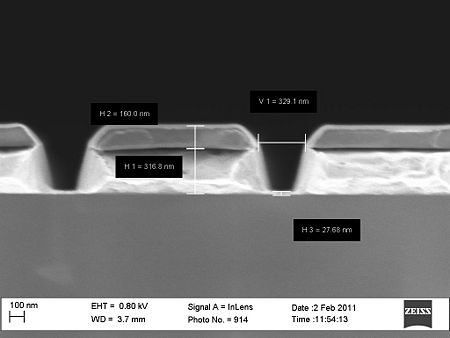
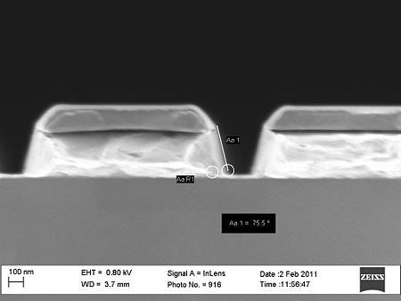
Some SEM profile images of the etched Au
 |
 |
|---|
THIS PAGE IS UNDER CONSTRUCTION
IBE Au etch with Ti mask
Work has been started to find a good process for etching gold with a Titanium mask with high selektivity.
| Method 1 | Method 2 | |
|---|---|---|
| Generel description | Generel description - method 1 | Generel description - method 2 |
| Parameter 1 |
|
|
| Parameter 2 |
|
|
| Substrate size |
|
|
| Allowed materials |
|
|
