Specific Process Knowledge/Lithography/Strip: Difference between revisions
Created page with "==Plasma asher 1 - ''All purpose''== 322 × 324px|thumb|The PlasmaAsher1 is placed in Cleanroom 3. The Plasma Asher1( 300 auto load model) can be u..." |
No edit summary |
||
| Line 1: | Line 1: | ||
==Plasma asher 1 | = Comparison table = | ||
{| border="2" cellspacing="0" cellpadding="2" | |||
!colspan="2" border="none" style="background:silver; color:black;" align="center"|Equipment | |||
|style="background:WhiteSmoke; color:black"|<b>[[Specific_Process_Knowledge/Lithography/UVExposure#KS Aligner|KS Aligner]]</b> | |||
|style="background:WhiteSmoke; color:black"|<b>[[Specific_Process_Knowledge/Lithography/UVExposure#EVG Aligner|EVG Aligner]]</b> | |||
|style="background:WhiteSmoke; color:black"|<b>[[Specific_Process_Knowledge/Lithography/UVExposure#III-V Aligner|III-V Aligner]]</b> | |||
|style="background:WhiteSmoke; color:black"|<b>[[Specific_Process_Knowledge/Lithography/UVExposure#Inclined UV Lamp|Inclined UV Lamp]]</b> | |||
|- | |||
!style="background:silver; width:100px; color:black;" align="center"|Purpose | |||
|style="background:LightGrey; color:black"| | |||
|style="background:WhiteSmoke; color:black"| | |||
*TS and BS Alignment | |||
*UV exposure | |||
|style="background:WhiteSmoke; color:black"| | |||
*TS and BS Alignment | |||
*UV exposure | |||
|style="background:WhiteSmoke; color:black"| | |||
*TS Alignment | |||
*UV exposure | |||
| | |||
|- | |||
!style="background:silver; color:black" align="center" valign="center" rowspan="3"|Performance | |||
|style="background:LightGrey; color:black"|Minimum feature size | |||
|style="background:WhiteSmoke; color:black"| | |||
*1.25µm down to 1.0µm | |||
|style="background:WhiteSmoke; color:black"| | |||
*1.25µm | |||
|style="background:WhiteSmoke; color:black"| | |||
| | |||
|- | |||
|style="background:LightGrey; color:black"|Exposure light/filters/spectrum | |||
|style="background:WhiteSmoke; color:black"| | |||
* 350W Hg-lamp, 365nm filter, 303nm filter optional | |||
* intensity in Constant Intensity(CI) mode 7mJ/cm2 | |||
|style="background:WhiteSmoke; color:black"| | |||
* 350W Hg-lamp, SU8 filter, 365nm filter optional | |||
* intensity in Constant Intensity(CI) mode 7mJ/cm2 | |||
|style="background:WhiteSmoke; color:black"| | |||
* | |||
|style="background:WhiteSmoke; color:black"| | |||
* | |||
|- | |||
|style="background:LightGrey; color:black"|Exposure mode | |||
|style="background:WhiteSmoke; color:black"| | |||
*proximity, soft, hard, vacuum contact | |||
|style="background:WhiteSmoke; color:black"| | |||
*proximity, soft, hard, vacuum contact | |||
*proximity, soft, hard, vacuum contact | |||
|style="background:WhiteSmoke; color:black"| | |||
* | |||
|style="background:WhiteSmoke; color:black"| | |||
* | |||
|- | |||
!style="background:silver; color:black" align="center" valign="center" rowspan="2"|Process parameter range | |||
|style="background:LightGrey; color:black"|Positive Process | |||
|style="background:WhiteSmoke; color:black"| | |||
* | |||
|style="background:WhiteSmoke; color:black"| | |||
* | |||
|style="background:WhiteSmoke; color:black"| | |||
* | |||
|style="background:WhiteSmoke; color:black"| | |||
* | |||
|- | |||
|style="background:LightGrey; color:black"|Negative Process | |||
|style="background:WhiteSmoke; color:black"| | |||
* | |||
|style="background:WhiteSmoke; color:black"| | |||
* | |||
|style="background:WhiteSmoke; color:black"| | |||
* | |||
|style="background:WhiteSmoke; color:black"| | |||
* | |||
|- | |||
!style="background:silver; color:black" align="center" valign="center" rowspan="3"|Substrates | |||
|style="background:LightGrey; color:black"|Batch size | |||
|style="background:WhiteSmoke; color:black"| | |||
*<nowiki>1</nowiki> small samples | |||
*<nowiki>1</nowiki> 50 mm wafers | |||
*<nowiki>1</nowiki> 100 mm wafers | |||
*<nowiki>1</nowiki> 150 mm wafers | |||
|style="background:WhiteSmoke; color:black"| | |||
*<nowiki>1</nowiki> 50 mm wafers | |||
*<nowiki>1</nowiki> 100 mm wafers | |||
*<nowiki>25</nowiki> 150 mm wafers with automatic handling | |||
|style="background:WhiteSmoke; color:black"| | |||
*<nowiki>1</nowiki> small samples | |||
*<nowiki>1</nowiki> 50 mm wafers | |||
*<nowiki>1</nowiki> 100 mm wafers | |||
*<nowiki>1</nowiki> 150 mm wafers | |||
|style="background:WhiteSmoke; color:black"| | |||
* | |||
|- | |||
| style="background:LightGrey; color:black"|Allowed materials | |||
|style="background:WhiteSmoke; color:black"| | |||
*Si and silicon oxide, silicon nitride | |||
*Quartz, pyrex | |||
|style="background:WhiteSmoke; color:black"| | |||
*Si and silicon oxide, silicon nitride | |||
*Quartz, pyrex | |||
|style="background:WhiteSmoke; color:black"| | |||
*III-V compounds | |||
|style="background:WhiteSmoke; color:black"| | |||
* | |||
|- | |||
|} | |||
<br clear="all" /> | |||
=Plasma asher 1 = | |||
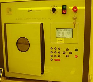
[[Image:plasmaasher2.JPG|322 × 324px|thumb|The PlasmaAsher1 is placed in Cleanroom 3.]] | [[Image:plasmaasher2.JPG|322 × 324px|thumb|The PlasmaAsher1 is placed in Cleanroom 3.]] | ||
| Line 17: | Line 136: | ||
==Overview of typical processes== | |||
{| border="2" cellspacing="0" cellpadding="4" align="left" | {| border="2" cellspacing="0" cellpadding="4" align="left" | ||
| Line 70: | Line 189: | ||
A typical process time for stripping of 1.5 µm AZ5214e resist is 15-25 min and for stripping of 9.5 µm AZ4562 resist is 20-35 min with the process parameters: 210ml O<math>_2</math>/min or mixture of 210ml O<math>_2</math>/min and 70ml N<math>_2</math>/min, power 1000W. | A typical process time for stripping of 1.5 µm AZ5214e resist is 15-25 min and for stripping of 9.5 µm AZ4562 resist is 20-35 min with the process parameters: 210ml O<math>_2</math>/min or mixture of 210ml O<math>_2</math>/min and 70ml N<math>_2</math>/min, power 1000W. | ||
=Plasma asher 2 = | |||
[[Image:Plasma_Asher_6inch.jpg|300x300px|thumb|Plasma asher for removing AZ resist on 6" wafers: positioned in cleanroom ? (class 10 yellow room)]] | [[Image:Plasma_Asher_6inch.jpg|300x300px|thumb|Plasma asher for removing AZ resist on 6" wafers: positioned in cleanroom ? (class 10 yellow room)]] | ||
| Line 113: | Line 232: | ||
<br clear="all" /> | <br clear="all" /> | ||
=Lift-off wet bench= | |||
[[Image:Acetone_lift-off.jpg|300x300px|thumb|Acetone lift-off: positioned in cleanroom 3]] | [[Image:Acetone_lift-off.jpg|300x300px|thumb|Acetone lift-off: positioned in cleanroom 3]] | ||
This bench is only for wafers with metal! | This bench is only for wafers with metal! | ||
| Line 125: | Line 244: | ||
<br clear="all" /> | <br clear="all" /> | ||
=Overview of acetone benches= | |||
{| border="2" cellspacing="0" cellpadding="4" align="left" | {| border="2" cellspacing="0" cellpadding="4" align="left" | ||
Revision as of 13:12, 9 August 2013
Comparison table
| Equipment | KS Aligner | EVG Aligner | III-V Aligner | Inclined UV Lamp | |
|---|---|---|---|---|---|
| Purpose |
|
|
|
||
| Performance | Minimum feature size |
|
|
||
| Exposure light/filters/spectrum |
|
|
|
| |
| Exposure mode |
|
|
|
| |
| Process parameter range | Positive Process |
|
|
|
|
| Negative Process |
|
|
|
| |
| Substrates | Batch size |
|
|
|
|
| Allowed materials |
|
|
|
| |
Plasma asher 1

The Plasma Asher1( 300 auto load model) can be used for the following process:
- Photoresist stripping
- Surface cleaning after storage
- Surface cleaning after processes using oil pump or diffusion pump vacuum
- Surface cleaning as part of photolithography after wet developing of lacquer structures prior to wet or plasma etching
- Stripping of photoresist layers after etching, including after being exposed to high temperatures as after implantation, ion etching, sputter etching, RIE
- Removal of organic passivating layers and masks
- Etching of glass and ceramic
- Etching of SiO, SiN, Si
- Removal of polyimide layers
The machine can be used for almost every materials, but if you have any doubt about your materials are compatible with the plasma process it is better to ask photolithography group at Danchip.
Overview of typical processes
| Photoresist stripping | Surface treatment of plastic, ceramic and metal | Ashing of organic material | |
|---|---|---|---|
| Process pressure | 0.8- 1.0mbar | 0.5- 1.0mbar | 0.8-1.5mbar |
| Process gases | O2, N2 | O, CF, N or their mixtures | O2 |
| Process power | 600-1000W | 150-300W | 1000W or less for heat- sensitive materials |
| Process time | 5-60min, depending of photoresist thickness | a few seconds to a few minutes | Between 0.5 and 20 hours, depending on the material |
| Batch size | 1-10 wafers at a time | 1 wafer at a time | 1 wafer at a time, use a container: Petri dish, evaporating dish weighing dish, beaker, etc. |
| Size of substrate | 2"-6" | 2"-6" | 2"-6" |
| Allowed materials | All | All | All |
A typical process time for stripping of 1.5 µm AZ5214e resist is 15-25 min and for stripping of 9.5 µm AZ4562 resist is 20-35 min with the process parameters: 210ml O/min or mixture of 210ml O/min and 70ml N/min, power 1000W.
Plasma asher 2

The Plasma Asher 2 is the same as Plasma Asher 1 but has another loading system which is more convenient for batch loading of 6inch substrates.
In this machine, only O2 and N2 gases are used for processes (in PlasmaAsher1, CF4 is used as well).
The typical process parameters when operating the equipment:
- Photeresist stripping
Pressure: 0.8 - 1.0 mbar
Gas: O2
Power: 600 - 1000 watts
Time: 5 -30 min., depending on photoresist type and thickness
A typical process time for stripping of 1.5 um AZ5214e resist is 25 min for 6 wafers load in a boat, recipe 1.
A Descum process in manuel mode:O2:70, N2:70, power:150W, time:10min Be sure to wait for cooling if the mashine has been used at 1000W right before. At a load at 2 Fused silicawafers resist removed 0.01-01,5um
The other materials have not been tested yet.
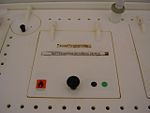
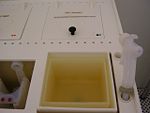
Acetone strip with ultrasound
 |
 |
This acetone strip is only for wafers without metal and SU-8!
There is two acetone bath: one rough for stripping the most of the resist from the surface and one fine with a ultrasound for cleaning the resists remains.
Here are the main rules for acetone strip use:
- Place the wafers in a wafer holder and put them in the first bath for 2-5 min, this time is depending how much resist you have on the surface.
- After the rough strip place your wafers directly in the final bath, switch on for the ultra sound and strip them for 2-3 min.
- Rinse your wafers for 4-5 min. in running water after stripping .
Lift-off wet bench

This bench is only for wafers with metal!
Here are the main rules for lift-off bench use:
- Place the wafers in a dedicated wafer holder.
- Put the holder in the acetone and start the ultrasound. The strip off time is depending of resist thickness.
- Rinse your wafers for 4-5 min. in running water after stripping.
Find more info about the lift-off process here: Specific Process Knowledge/Photolithography/AZ5214E standard resist - reverse process
Overview of acetone benches
| Acetone strip | Lift-off | |
|---|---|---|
| General description |
wet stripping of resist |
lift-off process |
| Chemical solution | CH3COCH3 | CH3COCH3 |
| Process temperature | 20 oC | 20 oC |
| Batch size |
1-25 wafers at a time |
1-25 wafer at a time |
| Size of substrate |
4" wafers |
4" wafers |
| Allowed materials |
|
|
