Specific Process Knowledge/Characterization/Optical characterization: Difference between revisions
| Line 10: | Line 10: | ||
Ellipsometry is an indirect measurement so a model has to be fit to the data in order to obtain the film thickness and optical constants. To learn more about ellipsometry you can take a look at the [http://www.jawoollam.com/tutorial_1.html tutorial] provided by the J. A. Woollam Co. | Ellipsometry is an indirect measurement so a model has to be fit to the data in order to obtain the film thickness and optical constants. To learn more about ellipsometry you can take a look at the [http://www.jawoollam.com/tutorial_1.html tutorial] provided by the J. A. Woollam Co. | ||
'''The user manual(s), quality control procedure(s) and results, user APV(s), technical information and contact information can be found in LabManager:''' | |||
<!-- remember to remove the type of documents that are not present --> | |||
<!-- give the link to the equipment info page in LabManager: --> | |||
[http://labmanager.danchip.dtu.dk/function.php?module=Machine&view=view&mach=18 LabManager] | |||
<br clear="all" /> | <br clear="all" /> | ||
===A rough overview of the performance of the Ellipsometers=== | ===A rough overview of the performance of the Ellipsometers=== | ||
Revision as of 13:14, 4 June 2013
Ellipsometer VASE and ellipsometer M2000-V 

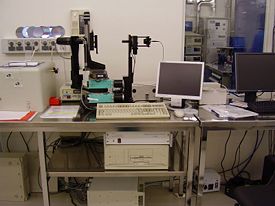
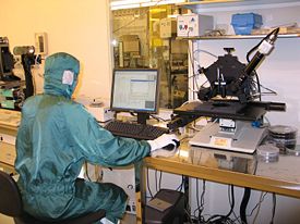
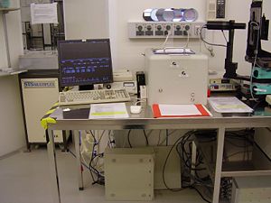
The ellipsometer VASE is a VASE (Variable Angle Spectroscopic Ellipsometry) ellipsometer from J.A. Woollam Co., Inc. The ellipsometer M2000V is a in-situ ellipsometer fraom J.A. Wollam Co., Inc. this is positioned on the Sputter System Lesker instrument for in-situ measurements.
Ellipsometry is a very sensitive characterization technique which can be used to determine thin film layer thicknesses and/or optical constants. It sends in polarized light on the surface at different angles and measures the change in polarization state of the reflected light.
It is especially good for thin films in the thickness range of a few nanometers to a few microns. The layer should be transparent to light in the usable wavelength range for the thickness to be determined. Large roughness (>40nm) and features within the field of view can cause the measurement to fail.
Ellipsometry is an indirect measurement so a model has to be fit to the data in order to obtain the film thickness and optical constants. To learn more about ellipsometry you can take a look at the tutorial provided by the J. A. Woollam Co.
The user manual(s), quality control procedure(s) and results, user APV(s), technical information and contact information can be found in LabManager:
A rough overview of the performance of the Ellipsometers
| Purpose | Film thickness measurements and optical characterization of optically transparent thin films |
|
|---|---|---|
| Performance | Thin film materials that can be measured |
Any film that is transparent to the light in the given wavelength range ex:
|
| Film thickness range |
| |
| Process parameter range | Wavelength range |
|
| Substrates | Batch size |
|
| Substrate material allowed |
|
Filmtek 4000

FilmTek 4000 is a computerized film thickness measurement and material characterization system. This system combines fiber-optic spectrophotometry with advanced material modeling software to provide an affordable and reliable tool for the simultaneous measurement of film thickness, index of refraction, and extinction coefficient
Normal incidence and polarized 70 degree reflection data is collected and used to calculate thickness and index of refraction of the measured film using SCI’s patented Differential Power Spectral Density (DPSD) technique. Absolute reflection data is obtained by comparing sample data to the measured reflection of a known reference sample, typically a silicon wafer with a thermally grown thin oxide (~63 nm) film.
The spectrophotometer scans the sample over a predefined range of wavelengths. The software generates a reflection spectrum based on a previously stored reference scan, and then performs a regression on the unknown parameters to fit the simulated reflection and power spectral density to the observed values. The resulting thin film parameters along with the measured and modeled spectra are then displayed for the user to examine.
An overview of the performance of the FilmTek
| Purpose | Film thickness measurements and optical characterization of optically transparent thin films |
|
|---|---|---|
| Performance | Thin film materials that can be measured |
Any film that is transparent to the light in the given wavelength range ex:
|
| Film thickness range |
| |
| Process parameter range | Wavelength range |
|
| Substrates | Batch size |
|
| Substrate material allowed |
|
Prism Coupler

The Prism coupler is a Metricon model 2010 Prism Coupler. It is an old system from 1991 but the system with a few modifications is still beening manufactured today. It is still a very easy and relaible method of determining thickness and refractive index. The prism coupler uses an optical waveguide technique to determine the thickness and refractive index of a thin film. To learn more about the theory of measurement please see the homepage of Metricon
It is especially good for making fast accurate measurements of dielectric thin films with n<2.02 and a thickness range of 1 µm to about 15 µm.
An overview of the performance of the Prism Coupler
| Purpose | Film thickness measurements and optical characterization of optically transparent thin films |
|
|---|---|---|
| Performance | Thin film materials that can be measured |
Film with a refractive index of less than 2.02 and that are transparent to the light in the given wavelength range ex:
|
| Film thickness range |
| |
| Film thickness accuracy |
| |
| Index accuracy |
| |
| Process parameter range | Wavelength range |
Can operate at two different wavelength:
|
| Substrates | Batch size |
|
| Substrate material allowed |
|
Comparison of the three methods
For comparison of the three methods, see here: Film thickness and optical constants of optical transparent films
