Specific Process Knowledge/Etch/ICP Metal Etcher/silicon/nano/nanoetch/211nmzep: Difference between revisions
Created page with "<gallery caption="The profiles of the 340 nm zep resist" widths="250" heights="200" perrow="3"> image:WF_2E02_mar23_2011-030.jpg|The 30 nm zep profile image:WF_2E02_mar23_2011..." |
No edit summary |
||
| (6 intermediate revisions by the same user not shown) | |||
| Line 1: | Line 1: | ||
'''Feedback to this page''': '''[mailto:labadviser@nanolab.dtu.dk?Subject=Feed%20back%20from%20page%20http://labadviser.nanolab.dtu.dk/index.php/Specific_Process_Knowledge/Etch/ICP_Metal_Etcher/silicon/nano/nanoetch/211nmzep click here]''' | |||
<!--Checked for updates on 30/7-2018 - ok/jmli --> | |||
<!--Checked for updates on 5/10-2020 - ok/jmli --> | |||
{{Template:Author-jmli1}} | |||
<!--Checked for updates on 2/02-2023 - ok/jmli --> | |||
<!--Checked for updates on 4/9-2025 - ok/jmli --> | |||
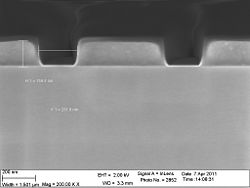
<gallery caption="The profiles of the 340 nm zep resist" widths="250" heights="200" perrow="3"> | <gallery caption="The profiles of the 340 nm zep resist" widths="250" heights="200" perrow="3"> | ||
image:WF_2E02_mar23_2011-030.jpg|The 30 nm zep profile | image:WF_2E02_mar23_2011-030.jpg|The 30 nm zep profile | ||
Latest revision as of 10:27, 4 September 2025
Feedback to this page: click here
Unless otherwise stated, all content on this page was created by Jonas Michael-Lindhard, DTU Nanolab
- The profiles of the 340 nm zep resist
-
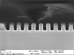 The 30 nm zep profile
 -
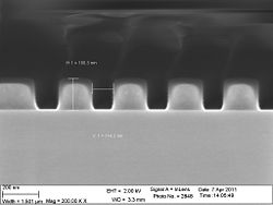 The 60 nm zep profile
 -
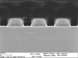 The 90 nm zep profile
 -
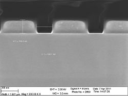 The 120 nm zep profile
 -
 The 150 nm zep profile


