Specific Process Knowledge/Characterization/Profiler/Optical Profiler (Sensofar) acceptance test: Difference between revisions
No edit summary |
|||
| (98 intermediate revisions by 4 users not shown) | |||
| Line 1: | Line 1: | ||
'''Feedback to this page''': '''[mailto:labadviser@nanolab.dtu.dk?Subject=Feed%20back%20from%20page%20http://labadviser.nanolab.dtu.dk/index.php/Specific_Process_Knowledge/Characterization/Profiler/Optical_Profiler_(Sensofar)_acceptance_test click here]''' | |||
=<span style="color:#FF0000"> This optical profiler has been decommissioned and replaced by the S Neox system, which is very similar </span> = | |||
=Results from the Optical Profiler (Sensofar) acceptance test= | =Results from the Optical Profiler (Sensofar) acceptance test= | ||
The acceptance test was performed in January 2012 by | The acceptance test was performed in January 2012 by ST Instruments and Sensofar together with | ||
Pernille V. Larsen @ | Pernille V. Larsen@ DTU nanolab and Berit G. Herstrøm @ DTU nanolab. | ||
==This Table shows the acceptance | ==This Table shows an overview of the acceptance tests== | ||
{| {{table} border="1" | {| {{table} border="1" | ||
| Line 12: | Line 16: | ||
| align="center" style="background:#f0f0f0;"|'''Acceptance criteria''' | | align="center" style="background:#f0f0f0;"|'''Acceptance criteria''' | ||
|- | |- | ||
| 1||Patterned flat sample of silicon||Sample material: Patterned silicon substrate | | [[#Results_of_acceptance_test_no._1,_2_and_3|1]]||Patterned flat sample of silicon||Sample material: Patterned silicon substrate <br/> Trench depth with aspect ratio 1:10 on a 10 µm wide trench||Depth 100±2 µm | ||
|- | |- | ||
| |||| | | |||||| | ||
|- | |- | ||
| 2||Patterned flat sample of silicon.||Sample material: Patterned silicon substrate | | [[#Results_of_acceptance_test_no._1,_2_and_3|2]]||Patterned flat sample of silicon.||Sample material: Patterned silicon substrate <br/> Trench depth with aspect ratio 1:11 on a 8 µm wide trench||Depth 91±2 µm | ||
|- | |- | ||
| |||| | | |||||| | ||
|- | |- | ||
| 3||Patterned flat sample of silicon||Sample material: Patterned silicon substrate||Depth 85±2 µm | | [[#Results_of_acceptance_test_no._1,_2_and_3|3]]||Patterned flat sample of silicon||Sample material: Patterned silicon substrate <br/> Trench depth with aspect ratio 1:13 on a 6.4 µm wide trench||Depth 85±2 µm | ||
|- | |- | ||
| |||| | | |||||| | ||
|- | |- | ||
| 4||Patterned flat sample of glass||3D profile of pattern etched down in a quartz sample.||Depth within ±1% from a standard profiler measurement and repeatability (3 successive measurements) within 0.1% | | [[#Results_of_acceptance_test_no._4|4]]||Patterned flat sample of glass||3D profile of pattern etched down in a quartz sample. <br/> Pattern size 20 µm x 20 µm, depth 500 nm||Depth within ±1% from a standard profiler measurement and repeatability (3 successive measurements) within 0.1% | ||
|- | |- | ||
| |||| | | |||||| | ||
|- | |- | ||
| 5||Flat sample of silicon with thick patterned oxide||Step height of patterned thick (10 µm) oxide on top of a silicon wafer.||Step height must be within ±3% of a SEM profile measurement. | | [[#Results of acceptance test no. 5|5]]||Flat sample of silicon with thick patterned oxide||Step height of patterned thick (10 µm) oxide on top of a silicon wafer. <br/> 7 µm deep pattern, trench width 6 µm||Step height must be within ±3% of a SEM profile measurement. | ||
|- | |- | ||
| |||| | | |||||| | ||
|- | |- | ||
| 6||Flat sample of silicon with thick layer of patterned polymer||Sample material: SU8 on silicon. ||Height 69±2 µm | | [[#Results of acceptance test no. 6|6]]||Flat sample of silicon with thick layer of patterned polymer||Sample material: SU8 on silicon. <br/> Pillar heights of 69 µm with 25 µm between pillar edges ||Height 69±2 µm | ||
|- | |- | ||
| |||| | | |||||| | ||
|- | |- | ||
| 7||Free standing structure||Measure bow due to stress of a membrane.||Membrane bow repeatability of 5 successive measurement within 2% | | [[#Results of acceptance test no. 7|7]]||Free standing structure||Measure bow due to stress of a membrane. <br/> Membrane material: Si(2 µm)/SiO2(~1 µm)/Au(50 nm) <br/> Membrane size: honey comb structure approximately 150 µm in diameter <br/> Bow < 500 nm ||Membrane bow repeatability of 5 successive measurement within 2% | ||
|- | |- | ||
| |||| | | |||||| | ||
|- | |- | ||
| |||| | | [[#Results of acceptance test no. 8|8]]||Stitching of large area||Stitching 4 mm x 4 mm on same sample as in 7. The area consists of many closed packed honey comb formed membranes.||Membrane bow must the same as on 7 within 2% | ||
|- | |- | ||
| |||| | | |||||| | ||
|- | |- | ||
| | | [[#Results of acceptance test no. 9|9]]||Narrow trenches and holes ||Sample material: Patterned silicon substrate <br/> 2.5 µm wide trench in silicon with a depth of 20 µm||Depth 20±2 µm | ||
|- | |- | ||
| | | |||||| | ||
|- | |- | ||
| |||| | | [[#Results of acceptance test no. 10|10]]||Film thickness measurement of transparent thin film||Transparent thin film thickness of 28 nm SiO2 on Si||SiO2 thickness 28±1 nm | ||
|- | |- | ||
| | | |||||| | ||
|- | |- | ||
| 11||Measurements of multiple stacks||120 nm nitride on 110 nm oxide on a silicon substrate||Within ±2% on each layer from an ellipsometer measurement. | | [[#Results of acceptance test no. 11|11]]||Measurements of multiple stacks||120 nm nitride on 110 nm oxide on a silicon substrate||Within ±2% on each layer from an ellipsometer measurement. | ||
|- | |- | ||
| | | |||||| | ||
|- | |- | ||
| ||||Measure thickness of AZ-resist on pillars of 50 µm in diameter|| | | [[#Results of acceptance test no. 12|12]]||Film thickness measurements of transparent films on small structure||Sample material: Si with 1.5 µm patterned AZ-resist <br/> Measure thickness of AZ-resist on pillars of 50 µm in diameter||Within ±1% from a standard profiler measurement. | ||
|- | |- | ||
| | | |||||| | ||
|- | |- | ||
| ||||3 successive measurements of the roughness || | | [[#Results of acceptance test no. 13|13]]||Roughness repeatability||Sample material: Si wafer with poly-silicon layer <br/> 3 successive measurements of the roughness ||Repeatability within 0.2% | ||
|- | |- | ||
|} | |} | ||
==Results of acceptance test no. 1, 2 and 3== | ==Results of acceptance test no. 1, 2 and 3== | ||
Sample material: Patterned silicon substrate | Sample material: Patterned silicon substrate | ||
Measurement: Trench depth with aspect ratio 1:10, 1:11 and 1:13 on a 10µm, 8mm and 6.4µm wide trenches respectively | Measurement: Trench depth with aspect ratio 1:10, 1:11 and 1:13 on a 10µm, 8mm and 6.4µm wide trenches respectively | ||
Acceptance criteria:Depth 100±2 µm, 91±2µm and 85±2µm. The SEM profile images of the three trenches are shown here: | |||
Acceptance criteria: Depth 100±2 µm, 91±2µm and 85±2µm. The SEM profile images of the three trenches are shown here: | |||
{| border="1" cellspacing="1" cellpadding="2" | {| border="1" cellspacing="1" cellpadding="2" | ||
! | ! | ||
[[image:Sensofar_A1_SEM.jpg| | [[image:Sensofar_A1_SEM.jpg|200x200px|thumb|center|A1]] | ||
! | ! | ||
[[image:Sensofar_A2_SEM.jpg| | [[image:Sensofar_A2_SEM.jpg|200x200px|thumb|center|A2]] | ||
! | ! | ||
[[image:Sensofar_A3_SEM.jpg| | [[image:Sensofar_A3_SEM.jpg|200x200px|thumb|center|A3]] | ||
|} | |} | ||
'''Results''' | |||
| Line 90: | Line 98: | ||
==== | ====Settings for methode no. 1 for test no. 1, 2 and 3: confocal==== | ||
Recipe: Trench | Recipe: Trench | ||
*Operation mode: trench | *Operation mode: trench | ||
| Line 99: | Line 107: | ||
**Dual - bottom up | **Dual - bottom up | ||
***top: 8µm | ***top: 8µm | ||
***Gap: 91µm (the trench depth) | ***Gap: 91µm (<- choose the trench depth) | ||
***Bottom: 8µm | ***Bottom: 8µm | ||
**Speed factor: 1x | **Speed factor: 1x | ||
| Line 113: | Line 121: | ||
*Objective: Interferometric 50x DI | *Objective: Interferometric 50x DI | ||
*Z scan: VSI | *Z scan: VSI | ||
*Light | *Light source: increased gain and contrast | ||
==Results of acceptance test no. 4== | ==Results of acceptance test no. 4== | ||
Sample material: Patterned | Sample material: Patterned flat sample of glass | ||
Measurement: Depth of pattern | Measurement: Depth of pattern | ||
Standard profiler measurement: | Standard profiler measurement:335 nm | ||
Acceptance criteria:Depth within ±1% from a standard profiler measurement (331.65nm-338.35nm) and repeatability (3 successive measurements) within 0.1% | Acceptance criteria:Depth within ±1% from a standard profiler measurement (331.65nm-338.35nm) and repeatability (3 successive measurements) within 0.1% | ||
| Line 126: | Line 134: | ||
'''System settings:''' | |||
Objective: DI 50x-N | Objective: DI 50x-N | ||
| Line 133: | Line 141: | ||
Treshold: 1% | Treshold: 1% | ||
Average 4 images (to reduce noise) | |||
| Line 146: | Line 156: | ||
| align="center" style="background:#f0f0f0;"|'''''' | | align="center" style="background:#f0f0f0;"|'''''' | ||
| align="center" style="background:#f0f0f0;"|'''Measured depth [nm]''' | | align="center" style="background:#f0f0f0;"|'''Measured depth [nm]''' | ||
| align="center" style="background:#f0f0f0;"|'''Repeated 20170925 with cover off''' | |||
| align="center" style="background:#f0f0f0;"|'''Repeated 20180816 after repair''' | |||
|- | |- | ||
| 1||337.5 | | 1||337.5||347.9||341.1 | ||
|- | |- | ||
| 2||336.5 | | 2||336.5||333.9||340.4 | ||
|- | |- | ||
| 3||334.7 | | 3||334.7||341.5||337.2 | ||
|- | |- | ||
| 4||335.5 | | 4||335.5||343.2||330.8 | ||
|- | |- | ||
| 5||339.2 | | 5||339.2||347.7||339.0 | ||
|- | |- | ||
| 6||337.2 | | 6||337.2||345.4||340.0 | ||
|- | |- | ||
| 7||334.2 | | 7||334.2||341.8||338.8 | ||
|- | |- | ||
| 8||335.5 | | 8||335.5||337.9||339.8 | ||
|- | |- | ||
| 9||341.1 | | 9||341.1||342.1||334.6 | ||
|- | |- | ||
| 10||344.4 | | 10||344.4||335.9||336.4 | ||
|- | |- | ||
|Average depth|| | |Average depth||337.58||341.73||337.82 | ||
|- | |- | ||
|Repeatability||3% (the bad repeatability was accepted due to the high noise level in the room) | |Repeatability||3.0% (the bad repeatability was accepted due to the high noise level in the room)||4.1%||3.0% | ||
|} | |} | ||
==Results of acceptance test no. 5== | ==Results of acceptance test no. 5== | ||
Sample: Flat sample of silicon with thick patterned oxide. | Sample: Flat sample of silicon with thick patterned oxide (APOX). | ||
Measurement: Step height of patterned thick (10 µm) oxide on top of a silicon wafer.The pattern is aprox. 7µm thick | Measurement: Step height of patterned thick (10 µm) oxide on top of a silicon wafer. The pattern is aprox. 7µm thick. | ||
Acceptance criteria: Step height must be within ±3% of a SEM profile measurement. See the SEM profile here: | Acceptance criteria: Step height must be within ±3% of a SEM profile measurement. See the SEM profile here: | ||
| Line 182: | Line 193: | ||
{| border="1" cellspacing="1" cellpadding="2" | {| border="1" cellspacing="1" cellpadding="2" | ||
! | ! | ||
[[Image:Sensofar_A5_SEM.jpg| | [[Image:Sensofar_A5_SEM.jpg|200x200px|thumb|center|A5]] | ||
|} | |} | ||
See the result here: | '''Settings:''' | ||
*Recipe: Acceptance nr. 5 SMR | |||
*Mode: default | |||
*Objective: 50x-DI | |||
*VSI Z scan 18.0µm | |||
*Threshold 2% | |||
*Note: Scan only in the APOX (not in the Si) or else the system will get confused. | |||
'''See the result here:''' | |||
{| border="1" cellspacing="1" cellpadding="2" | {| border="1" cellspacing="1" cellpadding="2" | ||
! | ! | ||
| Line 198: | Line 217: | ||
Acceptance criteria: Height 69±2 µm | Acceptance criteria: Height 69±2 µm | ||
'''Settings:''' | |||
*Recipe: Acceptance nr. 6 SMR | |||
*Mode: application Acceptance 6 | |||
**Raw smoothing confocal | |||
**Coarse shift single samle | |||
**Reject multiple reflections | |||
*Objective: Confocal EPI 20x-N | |||
*Z scan range: 104µm | |||
*Threshold: 2.0% | |||
'''See the result here:''' | |||
{| border="1" cellspacing="1" cellpadding="2" | |||
! | |||
[[Media:Sensofar_A6_20x.pdf|Sensofar A6 result no. 1 ]] | |||
! | |||
[[Media:Sensor_A6_20x_no2.pdf|Sensofar A6 result no. 2 ]] | |||
|} | |||
==Results of acceptance test no. 7== | |||
Sample: Free standing structure. Membrane material: Si(2 µm)/SiO2(~1 µm)/Au(50 nm). Membrane size: honey comb structure approximately 150 µm in diameter | |||
Measure: Measure bow due to stress of a membrane. | |||
Acceptance criteria: Membrane bow repeatability of 5 successive measurement within 2% | |||
The sample was not as we suspected. There was almost no bow. The membrane looked broken and it did not really make any sense to measure the bow. | |||
'''Settings:''' | |||
Two different setting were tried out, the second was the most successful: | |||
Setting no. 1: | |||
*Objective: DI 50x-N | |||
*PSI | |||
*Threshold 2% | |||
Setting no. 2: | |||
*Objective: DI 50x-N | |||
*Z scan: VSI 10µm | |||
*Threshold: 1.0% | |||
'''Result''' | |||
The measurement we did are shown here: | |||
{| border="1" cellspacing="1" cellpadding="2" | |||
! | |||
[[Media:Sensofar_A7_overview of the measurements.pdf|Sensofar A7 result ]] | |||
|} | |||
==Results of acceptance test no. 8== | |||
Measurement: Stitching 4 mm x 4 mm on same sample as in 7. | |||
Sample: The area consists of many closed packed honey comb formed membranes | |||
Acceptance criteria: Membrane bow must the same as on 7 within 2% | |||
'''Settings:''' | |||
*Extended topography | |||
*Objective: DI 20x-N | |||
*Z scan: VSI: 40µm | |||
*Threshold: 1.0% | |||
'''Result:''' | |||
We made a stitched image of the hole membrane and repeated it two times. It looked much the same but as for test 7 it was hard to do any measurements on it. See the images and profiles in the result file: | |||
{| border="1" cellspacing="1" cellpadding="2" | |||
! | |||
[[Media:Sensofar_A8_stitching_analysis_1_2.pdf|Sensofar A8 result ]] | |||
|} | |||
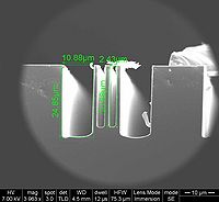
==Results of acceptance test no. 9== | |||
Sample: Patterned silicon substrate. | |||
Measurement: Narrow trench depth | |||
Acceptance criteria: 20±2µm, see the SEM images here: | |||
{| border="1" cellspacing="1" cellpadding="2" | |||
! | |||
[[image:Sensofar_A9_SEM.jpg|200x200px|thumb|center|SEM profile image of structure]] | |||
|} | |||
'''Setting''' | |||
Recipe: Narrow trench | |||
*Operation mode: narrow trench | |||
**Coarse shift single sampling | |||
*Objective: EPI 100X-N | |||
*Z scan: | |||
**Dual - bottom up | |||
***top: 4µm | |||
***Gap: 20µm (the trench depth) | |||
***Bottom: 4µm | |||
*Speed factor: 1x | |||
*Threshold: 0.0% | |||
*Light source: | |||
**Levels: 2 | |||
**176 -> 30 (might need to be set a little different) | |||
*Gain: default | |||
'''Result''' | |||
{| border="1" cellspacing="1" cellpadding="2" | |||
! | |||
[[Media:Sensofar_A9_narrow_trench.pdf|Sensofar A9 result ]] | |||
|} | |||
==Results of acceptance test no. 10== | |||
Sample: Transparent thin film thickness of 28 nm SiO2 on Si | |||
Measurement:Film thickness measurement of transparent thin film | |||
Acceptance criteria: SiO2 thickness 28±1 nm | |||
'''Settings''' | |||
*Objective: EPI 20x-N | |||
*Model: SiO2 thermal | |||
'''Result''' | |||
The result was 28.7nm | |||
==Results of acceptance test no. 11== | |||
Sample: 120 nm nitride on 110 nm oxide on a silicon substrate | |||
Measurement: Measurements of multiple stacks | |||
Acceptance criteria: Within ±2% on each layer from an ellipsometer measurement (SiO2: 112nm, Si3N4: 139nm) | |||
'''Settings''' | |||
Model layers use: | |||
*SiO2_(therm) | |||
*Si3N4 | |||
'''Result''' | |||
*SiO2: 113.1nm | |||
*Si3N4: 136.9nm | |||
==Results of acceptance test no. 12== | |||
Sample: Si with 1.4 µm patterned AZ-resist on 50µm pillars | |||
Measurement: Film thickness measurements of transparent films on small structure | |||
Acceptance criteria: Within ±1% from a standard profiler measurement. | |||
'''Settings''' | |||
Used Models -> Others -> Cauchy | |||
Options -> Roughness -> change amplitude fitting | |||
'''Result''' | |||
Within limits | |||
==Results of acceptance test no. 13== | |||
Sample: Si wafer with poly-silicon layer | |||
Measurement: Roughness repeatability, 3 successive measurements of the roughness | |||
Acceptance criteria: Repeatability within 0.2% | |||
Note: Because the surface roughness of the sample was very low and the noise/vibration level too high we could not obtain the specified repeatability. | |||
'''Result''' | |||
*The surface roughness (Ra) was 0.5nm | |||
*The repeatability over 10 measurements was 34% | |||
*The maximum deviation in roughness was 0.2nm | |||
Se the number in the file below: | |||
{| border="1" cellspacing="1" cellpadding="2" | |||
! | |||
[[Media:Sensofar_13_psi_1_average.pdf|Sensofar A13 result ]] | |||
|} | |||
Latest revision as of 10:27, 4 September 2025
Feedback to this page: click here
This optical profiler has been decommissioned and replaced by the S Neox system, which is very similar
Results from the Optical Profiler (Sensofar) acceptance test
The acceptance test was performed in January 2012 by ST Instruments and Sensofar together with Pernille V. Larsen@ DTU nanolab and Berit G. Herstrøm @ DTU nanolab.
This Table shows an overview of the acceptance tests
| ' | Title | Sample description / measurement | Acceptance criteria |
| 1 | Patterned flat sample of silicon | Sample material: Patterned silicon substrate Trench depth with aspect ratio 1:10 on a 10 µm wide trench |
Depth 100±2 µm |
| 2 | Patterned flat sample of silicon. | Sample material: Patterned silicon substrate Trench depth with aspect ratio 1:11 on a 8 µm wide trench |
Depth 91±2 µm |
| 3 | Patterned flat sample of silicon | Sample material: Patterned silicon substrate Trench depth with aspect ratio 1:13 on a 6.4 µm wide trench |
Depth 85±2 µm |
| 4 | Patterned flat sample of glass | 3D profile of pattern etched down in a quartz sample. Pattern size 20 µm x 20 µm, depth 500 nm |
Depth within ±1% from a standard profiler measurement and repeatability (3 successive measurements) within 0.1% |
| 5 | Flat sample of silicon with thick patterned oxide | Step height of patterned thick (10 µm) oxide on top of a silicon wafer. 7 µm deep pattern, trench width 6 µm |
Step height must be within ±3% of a SEM profile measurement. |
| 6 | Flat sample of silicon with thick layer of patterned polymer | Sample material: SU8 on silicon. Pillar heights of 69 µm with 25 µm between pillar edges |
Height 69±2 µm |
| 7 | Free standing structure | Measure bow due to stress of a membrane. Membrane material: Si(2 µm)/SiO2(~1 µm)/Au(50 nm) Membrane size: honey comb structure approximately 150 µm in diameter Bow < 500 nm |
Membrane bow repeatability of 5 successive measurement within 2% |
| 8 | Stitching of large area | Stitching 4 mm x 4 mm on same sample as in 7. The area consists of many closed packed honey comb formed membranes. | Membrane bow must the same as on 7 within 2% |
| 9 | Narrow trenches and holes | Sample material: Patterned silicon substrate 2.5 µm wide trench in silicon with a depth of 20 µm |
Depth 20±2 µm |
| 10 | Film thickness measurement of transparent thin film | Transparent thin film thickness of 28 nm SiO2 on Si | SiO2 thickness 28±1 nm |
| 11 | Measurements of multiple stacks | 120 nm nitride on 110 nm oxide on a silicon substrate | Within ±2% on each layer from an ellipsometer measurement. |
| 12 | Film thickness measurements of transparent films on small structure | Sample material: Si with 1.5 µm patterned AZ-resist Measure thickness of AZ-resist on pillars of 50 µm in diameter |
Within ±1% from a standard profiler measurement. |
| 13 | Roughness repeatability | Sample material: Si wafer with poly-silicon layer 3 successive measurements of the roughness |
Repeatability within 0.2% |
Results of acceptance test no. 1, 2 and 3
Sample material: Patterned silicon substrate
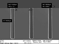
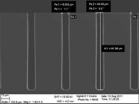
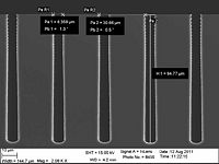
Measurement: Trench depth with aspect ratio 1:10, 1:11 and 1:13 on a 10µm, 8mm and 6.4µm wide trenches respectively
Acceptance criteria: Depth 100±2 µm, 91±2µm and 85±2µm. The SEM profile images of the three trenches are shown here:
 |
 |
 |
|---|
Results
Test no. 1 was done in two ways:
- With confocal objective EPI 100x-N: See the results here
- With Interferometric objective 50X DI: See the results here
Test no. 2 was done using: confocal objective EPI 100x-N: See the results here
Test no. 3 was done using: confocal objective EPI 100x-N: See the results here
Settings for methode no. 1 for test no. 1, 2 and 3: confocal
Recipe: Trench
- Operation mode: trench
- + Raw smoothing confocal
- + fine shift
- Objective: EPI 100X-N
- Z scan
- Dual - bottom up
- top: 8µm
- Gap: 91µm (<- choose the trench depth)
- Bottom: 8µm
- Speed factor: 1x
- + Linear stage
- Dual - bottom up
- Threshold: 0.0%
- Light source
- Levels: 2
- 900 -> 60 (might need to be set a little different)
- Gain: default
- Levels: 2
Setting for methode no. 2 for test no. 1: interferometric
We do not have a recipe for that but we used:
- Objective: Interferometric 50x DI
- Z scan: VSI
- Light source: increased gain and contrast
Results of acceptance test no. 4
Sample material: Patterned flat sample of glass
Measurement: Depth of pattern
Standard profiler measurement:335 nm
Acceptance criteria:Depth within ±1% from a standard profiler measurement (331.65nm-338.35nm) and repeatability (3 successive measurements) within 0.1%
System settings:
Objective: DI 50x-N
VSI z scan: 10µm
Treshold: 1%
Average 4 images (to reduce noise)
Results
It was repeated 10 Time.
The first measurement is shown here
This table show the depth value for the 10 measurements
| ' | Measured depth [nm] | Repeated 20170925 with cover off | Repeated 20180816 after repair |
| 1 | 337.5 | 347.9 | 341.1 |
| 2 | 336.5 | 333.9 | 340.4 |
| 3 | 334.7 | 341.5 | 337.2 |
| 4 | 335.5 | 343.2 | 330.8 |
| 5 | 339.2 | 347.7 | 339.0 |
| 6 | 337.2 | 345.4 | 340.0 |
| 7 | 334.2 | 341.8 | 338.8 |
| 8 | 335.5 | 337.9 | 339.8 |
| 9 | 341.1 | 342.1 | 334.6 |
| 10 | 344.4 | 335.9 | 336.4 |
| Average depth | 337.58 | 341.73 | 337.82 |
| Repeatability | 3.0% (the bad repeatability was accepted due to the high noise level in the room) | 4.1% | 3.0% |
Results of acceptance test no. 5
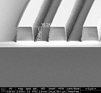
Sample: Flat sample of silicon with thick patterned oxide (APOX).
Measurement: Step height of patterned thick (10 µm) oxide on top of a silicon wafer. The pattern is aprox. 7µm thick.
Acceptance criteria: Step height must be within ±3% of a SEM profile measurement. See the SEM profile here:
 |
|---|
Settings:
- Recipe: Acceptance nr. 5 SMR
- Mode: default
- Objective: 50x-DI
- VSI Z scan 18.0µm
- Threshold 2%
- Note: Scan only in the APOX (not in the Si) or else the system will get confused.
See the result here:
Results of acceptance test no. 6
Sample: Flat sample of silicon with thick layer of patterned SU8.
Measure: step height.
Acceptance criteria: Height 69±2 µm
Settings:
- Recipe: Acceptance nr. 6 SMR
- Mode: application Acceptance 6
- Raw smoothing confocal
- Coarse shift single samle
- Reject multiple reflections
- Objective: Confocal EPI 20x-N
- Z scan range: 104µm
- Threshold: 2.0%
See the result here:
Results of acceptance test no. 7
Sample: Free standing structure. Membrane material: Si(2 µm)/SiO2(~1 µm)/Au(50 nm). Membrane size: honey comb structure approximately 150 µm in diameter
Measure: Measure bow due to stress of a membrane.
Acceptance criteria: Membrane bow repeatability of 5 successive measurement within 2%
The sample was not as we suspected. There was almost no bow. The membrane looked broken and it did not really make any sense to measure the bow.
Settings: Two different setting were tried out, the second was the most successful:
Setting no. 1:
- Objective: DI 50x-N
- PSI
- Threshold 2%
Setting no. 2:
- Objective: DI 50x-N
- Z scan: VSI 10µm
- Threshold: 1.0%
Result
The measurement we did are shown here:
Results of acceptance test no. 8
Measurement: Stitching 4 mm x 4 mm on same sample as in 7.
Sample: The area consists of many closed packed honey comb formed membranes
Acceptance criteria: Membrane bow must the same as on 7 within 2%
Settings:
- Extended topography
- Objective: DI 20x-N
- Z scan: VSI: 40µm
- Threshold: 1.0%
Result:
We made a stitched image of the hole membrane and repeated it two times. It looked much the same but as for test 7 it was hard to do any measurements on it. See the images and profiles in the result file:
Results of acceptance test no. 9
Sample: Patterned silicon substrate.
Measurement: Narrow trench depth
Acceptance criteria: 20±2µm, see the SEM images here:
 |
|---|
Setting
Recipe: Narrow trench
- Operation mode: narrow trench
- Coarse shift single sampling
- Objective: EPI 100X-N
- Z scan:
- Dual - bottom up
- top: 4µm
- Gap: 20µm (the trench depth)
- Bottom: 4µm
- Dual - bottom up
- Speed factor: 1x
- Threshold: 0.0%
- Light source:
- Levels: 2
- 176 -> 30 (might need to be set a little different)
- Gain: default
Result
Results of acceptance test no. 10
Sample: Transparent thin film thickness of 28 nm SiO2 on Si
Measurement:Film thickness measurement of transparent thin film
Acceptance criteria: SiO2 thickness 28±1 nm
Settings
- Objective: EPI 20x-N
- Model: SiO2 thermal
Result
The result was 28.7nm
Results of acceptance test no. 11
Sample: 120 nm nitride on 110 nm oxide on a silicon substrate
Measurement: Measurements of multiple stacks
Acceptance criteria: Within ±2% on each layer from an ellipsometer measurement (SiO2: 112nm, Si3N4: 139nm)
Settings Model layers use:
- SiO2_(therm)
- Si3N4
Result
- SiO2: 113.1nm
- Si3N4: 136.9nm
Results of acceptance test no. 12
Sample: Si with 1.4 µm patterned AZ-resist on 50µm pillars
Measurement: Film thickness measurements of transparent films on small structure
Acceptance criteria: Within ±1% from a standard profiler measurement.
Settings
Used Models -> Others -> Cauchy
Options -> Roughness -> change amplitude fitting
Result
Within limits
Results of acceptance test no. 13
Sample: Si wafer with poly-silicon layer
Measurement: Roughness repeatability, 3 successive measurements of the roughness
Acceptance criteria: Repeatability within 0.2%
Note: Because the surface roughness of the sample was very low and the noise/vibration level too high we could not obtain the specified repeatability.
Result
- The surface roughness (Ra) was 0.5nm
- The repeatability over 10 measurements was 34%
- The maximum deviation in roughness was 0.2nm
Se the number in the file below:
