Specific Process Knowledge/Etch/DRIE-Pegasus/Pegasus-4/SiO2 Etch: Difference between revisions
No edit summary |
No edit summary |
||
| Line 50: | Line 50: | ||
<br clear="all"/> | <br clear="all"/> | ||
==SiO2 etch with Cr mask== | ==SiO2 etch with Cr mask== | ||
| Line 183: | Line 145: | ||
File:C09721_center_21.jpg | File:C09721_center_21.jpg | ||
File:C09721_center_22.jpg | File:C09721_center_22.jpg | ||
</gallery> | |||
==SiO2 Etch using aSi as masking material== | |||
{{CC-bghe2}} <br> | |||
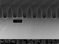
I was starting up development of SiO2 etch using aSi as masking material. This is on pause because the results did not look promishing on high aspect ratio structures wit DUV pattern due to large faceting on the aSi mask. I turned to Cr mask instead <br> | |||
The samples I use are: | |||
*6" Si afters with oxide (2µm), | |||
*aSi (~300nm), | |||
*Neg. DUV reist (~60nm barc, ~350 nm resist) | |||
*Reticle: Danchip/Triple-D | |||
*Dose 230 J/m2 | |||
First I need to make sure that the resist work for pattering the aSi layer is good. If the resist is not good the final etch will also not be good. | |||
===DUV optimization=== | |||
Dose test with the doses (J/m2): 200, 210, 220, 230, 240, 250, 270, 280 | |||
The aim was to get good line for 400nm pitch/200nm lines | |||
<gallery caption="400nm pitch 200 nm lines" perrow="5" widths="200px" heights="150px"> | |||
Image:dose200_no2_22.jpg |200 J/m2 400nm/268nm | |||
Image:dose210_no2_15.jpg |210 J/m2 400nm/239nm | |||
Image:dose220_no2_13.jpg |220 J/m2 400nm/208nm | |||
Image:dose230_no2_11.jpg |230 J/m2 400nm/209nm | |||
Image:dose240_no2_05.jpg |240 J/m2 400nm/215nm | |||
Image:dose250_no2_11.jpg |250 J/m2 400nm/207nm | |||
Image:dose260_no2_18.jpg |260 J/m2 400nm/188nm | |||
Image:dose270_no2_24.jpg |270 J/m2 400nm/155nm | |||
Image:dose280_no1_15.jpg |280 J/m2 400nm/0nm | |||
</gallery> | |||
<gallery caption="1000nm pitch 500 nm lines" perrow="3" widths="200px" heights="150px"> | |||
Image:dose210_no2_17.jpg |210 J/m2 1000nm/581nm | |||
Image:dose230_no2_12.jpg |230 J/m2 1000nm/517nm | |||
Image:dose240_no2_03.jpg |240 J/m2 1000nm/518nm | |||
Image:dose250_no2_09.jpg |250 J/m2 1000nm/510nm | |||
Image:dose260_no2_15.jpg |260 J/m2 1000nm/493nm | |||
Image:dose270_no2_22.jpg |270 J/m2 1000nm/494nm | |||
</gallery> | </gallery> | ||
Latest revision as of 12:45, 7 April 2026
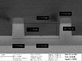
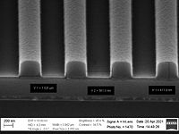
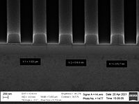
SiO2 Etch using resist as masking material
Unless otherwise stated, all content in this section was done by Berit Herstrøm, DTU Nanolab
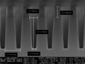
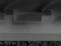
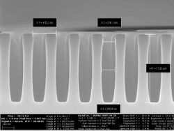
I have do some development of a SiO2 etch with resist as masking material. I have found this fairly good recipe. For now it is the standard SiO2 etch recipes but I might change the "Standard recipe" a a later time if I find a better one. If you need to etch deeper than 1 micrometer then I advise you to split the etch in several runs with O2 cleans in between (3min TDESC Clean) or else it seems like the the etch rate is going down over time.
- Recipe name: SiO2_res_10, Recipe no. 10: C06445_02 coil_2500W, platen:300W, He/C4F8= 17.5, C4F8/H2=1, Pressure:8.8mTorr, C4F8:25.6sccm, He:448.7sccm, H2:25.6sccm, 3:56 min
-
 0.4µ/0.2µ
Bad lithography -
 0.5/0.25µ
Etch depth: 652 nm
Resist left: 456 nm -
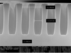
 1µ/0.5µ:
Etch depth: 855 nm
Resist left: 487 nm -
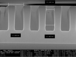
 2µ/1µ:
Etch depth: 952 nm
Resist left: 487 nm -
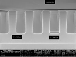
 4µ/2µ:
Etch depth: 1106 nm
Resist left: 487 nm -
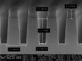
 0.8µ/0.2µ
Etch depth: 867 nm
Resist left: 426 nm -
 1.0µ/0.25µ:
Etch depth: 893 nm
Resist left: 460 nm -
 4µ/1µ:
Etch depth: 1033 nm
Resist left: 473 nm


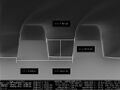
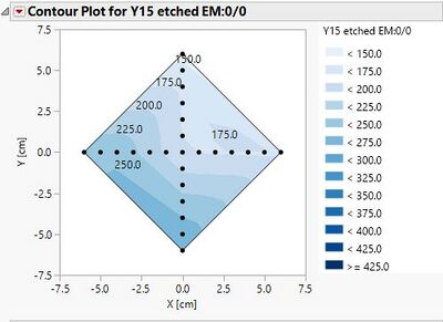
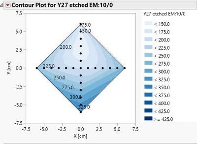
Uniformity results with SiO2_res_10

Results with SiO2_res_10 and with with the electro magnets on
The SiO2:res_10 recipe was tested with the electromagnets on but it seems to no no good for the results.

- Recipe name: SiO2_res_10, Recipe no. 10+EM coils: C06445_02 coil_2500W, platen:300W, EM:02/30A, He/C4F8= 17.5, C4F8/H2=1, Pressure:8.8mTorr, C4F8:25.6sccm, He:448.7sccm, H2:25.6sccm, 3:56 min
-
-
-
-
-


Using the electromagnetic coil on the recipe SiO2_res_10 gave higher etch rate on this chip, which is positioned in the center of a 6" wafer. The Etch profile is more angled.
- Removing the H2 from the recipe to get less redeposition at lower platen power (200W), EM:02/30A. Se result below. This gave significantly lower etch rate and no etching in the smallest openings.
- Recipe name: SiO2_res, Recipe no. 10+EM+edit coils: C09975 coil_2500W, platen:200W, EM:02/30A, Pressure:8.8mTorr, C4F8:25.6sccm, He:448.7sccm, H2:0sccm, 3:56 min
-
-
-
-
-


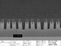
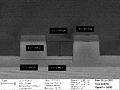
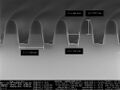
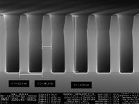
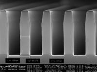
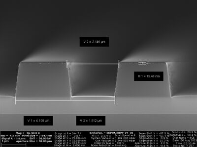
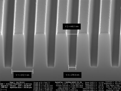
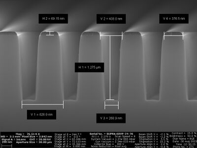
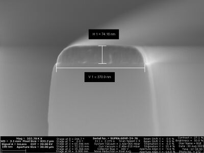
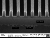
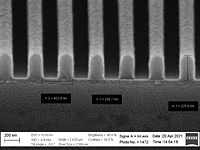
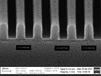
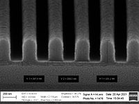
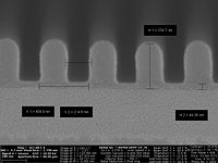
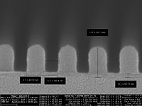
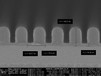
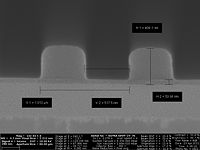
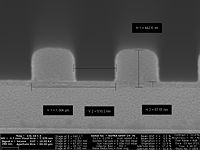
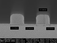
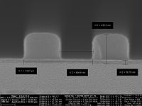
SiO2 etch with Cr mask
Unless otherwise stated, all content in this section was done by Berit Herstrøm, DTU Nanolab
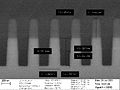
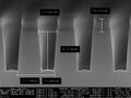
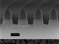
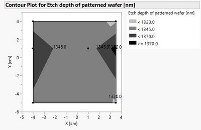
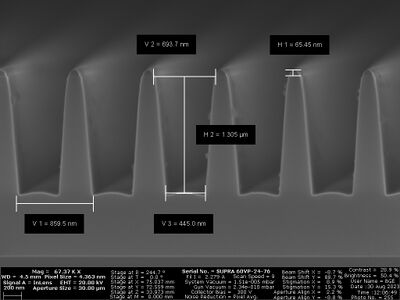
SiO2 etch with Cr mask 100 nm and with 500 nm for the resist for the Cr etch
Barc etch and Cr etch were done in ICP metal using end point detection. The sample was a full 6" wafer
- SiO2_res_10 2x5:00 min with 3 min TDESC clean in between 100 nm Cr mask, with 500 nm resist
-
-
-
-
-
-


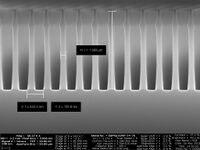
- SiO2_res_10 5:00 min 100 nm Cr mask, with 500 nm resist, resist/Cr stripped after etch in plasma asher 35min
-
 200nm/400nm
 -
 250nm/500nm
 -
 400nm/800nm
 -
 500nm/1000nm
 -
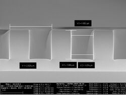 1000nm/2000nm
 -
 2000nm/4000nm


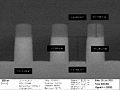
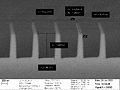
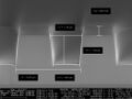
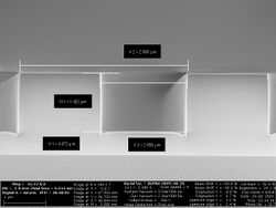
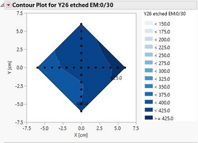
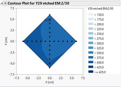
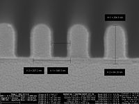
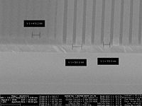
Testing with electromagnetic coils /Cr mask
Unless otherwise stated, all content in this section was done by Berit Herstrøm, DTU Nanolab
When testing with decreased platen power on the SiO2_10 standard recipe the uniformity got very bad. I then tested with the electromagnetics coil to see if that could affect the uniformity. There is an outer coil that can be varied between 0 A and 10 A and an inner coil that can be varied between 0 A and 30 A. The first tests were done on Si/SiO2(1µm) without pattern and measured on the ellipsometer.
| Parameter | Recipe name: no 10 with lower platen power |
|---|---|
| Coil Power [W] | 2500 |
| Platen Power [W] | 200 |
| Platen temperature [oC] | 20 |
| H2 flow [sccm] | 25.6 |
| C4F8 flow [sccm] | 25.6 |
| He flow [sccm] | 448.7 |
| Pressure | Fully open APC valve (8-9 mTorr) |
| Electromagnetic coils (EM) 'outer coil' / 'inner coil' | '0-10 A' / '0-30 A' |
- EM tests
-
 Etch time: 2 min, Average etch rate: 100.2 nm/min, range:+-55.1%
 -
 Etch time: 2 min, Average etch rate: 100.5 nm/min, range:+-32.6%
 -
 Etch time: 2 min, Average etch rate: 100.8 nm/min, range:+-50.8%
 -
 Etch time: 2 min, Average etch rate: 203.8 nm/min, range:+-6.1%
 -
 Etch time: 2 min, Average etch rate: 186.2 nm/min, range:+-3.2%
 -
 Etch time: 6 min on patterned wafer with different measurement points, <100 nm Cr mask is still on, EM_2/30, Average etch rate: 207-223 nm/min depending on how much Cr mask is left, range:+-2.3%


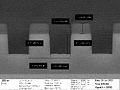
- EM tests with Cr mask on full wafer 6 min etch
-
-
-
-
-
-


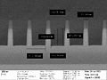
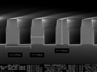
SiO2 Etch using aSi as masking material
Unless otherwise stated, all content in this section was done by Berit Herstrøm, DTU Nanolab
I was starting up development of SiO2 etch using aSi as masking material. This is on pause because the results did not look promishing on high aspect ratio structures wit DUV pattern due to large faceting on the aSi mask. I turned to Cr mask instead
The samples I use are:
- 6" Si afters with oxide (2µm),
- aSi (~300nm),
- Neg. DUV reist (~60nm barc, ~350 nm resist)
- Reticle: Danchip/Triple-D
- Dose 230 J/m2
First I need to make sure that the resist work for pattering the aSi layer is good. If the resist is not good the final etch will also not be good.
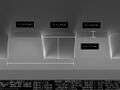
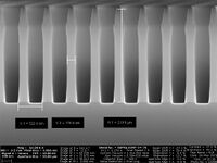
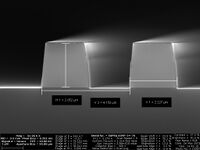
DUV optimization
Dose test with the doses (J/m2): 200, 210, 220, 230, 240, 250, 270, 280 The aim was to get good line for 400nm pitch/200nm lines
- 400nm pitch 200 nm lines
-
 200 J/m2 400nm/268nm
 -
 210 J/m2 400nm/239nm
 -
 220 J/m2 400nm/208nm
 -
 230 J/m2 400nm/209nm
 -
 240 J/m2 400nm/215nm
 -
 250 J/m2 400nm/207nm
 -
 260 J/m2 400nm/188nm
 -
 270 J/m2 400nm/155nm
 -
 280 J/m2 400nm/0nm


- 1000nm pitch 500 nm lines
-
 210 J/m2 1000nm/581nm
 -
 230 J/m2 1000nm/517nm
 -
 240 J/m2 1000nm/518nm
 -
 250 J/m2 1000nm/510nm
 -
 260 J/m2 1000nm/493nm
 -
 270 J/m2 1000nm/494nm


