Specific Process Knowledge/Etch/DRIE-Pegasus/Pegasus-3/SiO2 etch: Difference between revisions
No edit summary |
|||
| (4 intermediate revisions by the same user not shown) | |||
| Line 2: | Line 2: | ||
Pegasus 3 is not meant to be used as an SiO2 etcher. Please do not develop SiO2 recipes on this machine. Often SiO2 etch recipes are very polymerizing and that can disturb the chamber conditions for the silicon etching recipes. | Pegasus 3 is not meant to be used as an SiO2 etcher. Please do not develop SiO2 recipes on this machine. Often SiO2 etch recipes are very polymerizing and that can disturb the chamber conditions for the silicon etching recipes. | ||
The recipe developed here is only for etching through a very thin SiO2 layer and does not have a high selectivity to silicon to avoid the recipe | The recipe developed here is only for etching through a very thin SiO2 layer and does not have a high selectivity to silicon. This is to avoid the recipe from becoming too polymerizing. It is also not very uniform over the wafer, so when it is used for etching down to silicon it will also etch a lot in the silicon and in areas more than other. | ||
==Test work done== | ==Test work done== | ||
| Line 28: | Line 28: | ||
|} | |} | ||
{| class="wikitable" | |||
|+ Etch uniformity | |||
File:Peg3 SiO2 uniformity Y34 to Y40.jpg | |- | ||
File:Peg3 SiO2 uniformity normalized Y34 to Y40.jpg | ! SiO2 etch rate uniformity !! SiO2 etch rate uniformity normalized to center!! Si Etch rate uniformity | ||
File:Peg3 Si etch uniformity Y38 and Y40.jpg | |- | ||
| [[File:Peg3 SiO2 uniformity Y34 to Y40.jpg]] || [[File:Peg3 SiO2 uniformity normalized Y34 to Y40.jpg]] || valign="top"| [[File:Peg3 Si etch uniformity Y38 and Y40.jpg]] | |||
|} | |||
Latest revision as of 12:34, 5 February 2026
Etching of very thin layer of SiO2
Pegasus 3 is not meant to be used as an SiO2 etcher. Please do not develop SiO2 recipes on this machine. Often SiO2 etch recipes are very polymerizing and that can disturb the chamber conditions for the silicon etching recipes.
The recipe developed here is only for etching through a very thin SiO2 layer and does not have a high selectivity to silicon. This is to avoid the recipe from becoming too polymerizing. It is also not very uniform over the wafer, so when it is used for etching down to silicon it will also etch a lot in the silicon and in areas more than other.
Test work done
Unless otherwise stated, all content in this section was done by Berit Herstrøm, DTU Nanolab
The tests were done on 6" wafers. Silicon wafers with 1µm thermal SiO2 and mask less. Measurements were done on the ellipsometer before at after the etch to map the etch rate.
| Wafer number | C4F8 | SF6 flow | Ar | Platen power | Pressure | SiO2 Uniformity results | SiO2 Center Etch rate | Si Center Etch rate | Si Uniformity |
|---|---|---|---|---|---|---|---|---|---|
| Y34 | 50 sccm | 50 sccm | 0 sccm | 100 W | 80 mTorr | ±23.3% | 36.0 nm/min (highest) | ||
| Y35 | 25 sccm | 75 sccm | 0 sccm | 100 W | 80 mTorr | ±20.8% | 41.3 nm/min (highest) | ||
| Y36 | 25 sccm | 75 sccm | 0 sccm | 100 W | 10 mTorr | ±22.1% | 36.2 nm/min (lowest) | ||
| Y37 | 25 sccm | 75 sccm | 0 sccm | 100 W | 40 mTorr | ±24.6% | 24.4 nm/min (lowest) | ||
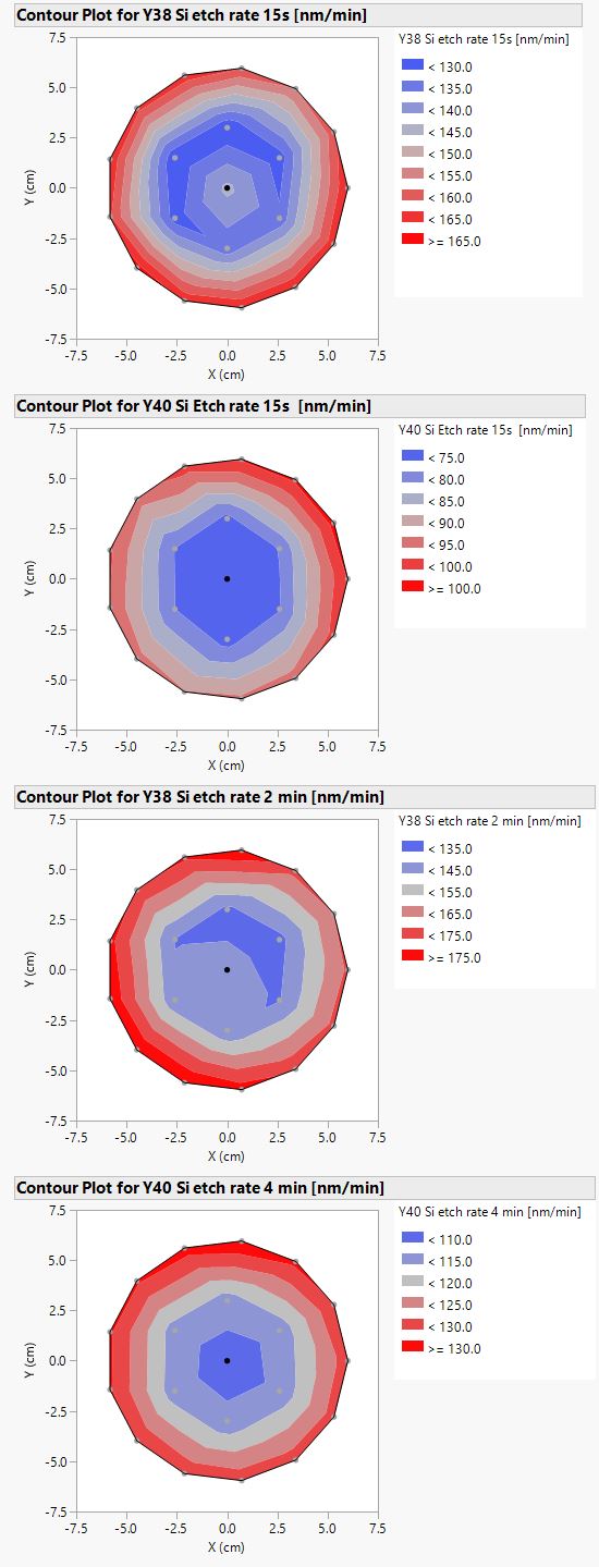
| Y38 | 25 sccm | 75 sccm | 0 sccm | 100 W | 60 mTorr | ± 8.1% | 34.0 nm/min (highest in center and at edge) | 141.4@15s, 137.5@2min | ± 13.9%@15s, ± 16.5%@2min |
| Y39 | 50 sccm | 150 sccm | 0 sccm | 100 W | 10 mTorr | ±25.0% | 34.8 nm/min (lowest) | ||
| Y40 | 8.33 sccm | 50 sccm | 100 sccm | 100 W | 10 mTorr | ±15.1% | 35.8 n/min (lowest) | 70.8@15s, 107.5@5min | ± 17.6%@15s, ± 11.1%@4min |
| SiO2 etch rate uniformity | SiO2 etch rate uniformity normalized to center | Si Etch rate uniformity |
|---|---|---|
 |
 |

|
