Specific Process Knowledge/Lithography/EBeamLithography/JEOLAlignment: Difference between revisions
| (66 intermediate revisions by the same user not shown) | |||
| Line 1: | Line 1: | ||
'''Feedback to this page''': '''[mailto:labadviser@nanolab.dtu.dk?Subject=Feed%20back%20from%20page%20http://labadviser.nanolab.dtu.dk/index.php/Specific_Process_Knowledge/Lithography/EBeamLithography/JEOLAlignment click here]''' | |||
Content and illustration by Thomas Pedersen, DTU Nanolab unless otherwise noted. | |||
=Aligned exposure on JEOL 9500= | =Aligned exposure on JEOL 9500= | ||
There is quite a few things to remember in order to align an exposure to an existing pattern. The example below is a step by step guide illustrating global substrate alignment as well as chip alignment. If your job only requires global alignment simply skip the chip alignment part. In the example we assume a layer, L1, is already defined on the substrate and the goal is to align the next layer, L2, to it. | There is quite a few things to remember in order to align an exposure to an existing pattern. The example below is a step by step guide illustrating global substrate alignment as well as chip alignment. If your job only requires global alignment simply skip the chip alignment part. In the example we assume a layer, L1, is already defined on the substrate and the goal is to align the next layer, L2, to it. | ||
The job is also explained in a [https://youtu.be/-wZpUNAq8dA?si=6pXad4WUPlKCfJJX&t=857 tutorial video found here.] | |||
==Job preparation== | ==Job preparation== | ||
| Line 13: | Line 20: | ||
|} | |} | ||
The following SDF and JDF files will be used for the example. | The following SDF and JDF files will be used for the example. Global alignment is initiated with the '''GLMDET''' command, which in this example is set to '''A''' for automatic. Chip alignment is also initiated with the '''CHIPAL''' command using a single chip mark. The sample reference height detection is set to height detection on each chip mark with the '''HSWITCH OFF,ON''' command. Global mark positions are stated in the JDF using the '''GLMPOS''' command and chip marks are defined using the '''CHMPOS''' command. | ||
<pre> | <pre> | ||
;SDF | ;SDF | ||
MAGAZIN 'THOPE' | MAGAZIN 'THOPE' | ||
# | #7 | ||
% | %4D | ||
JDF 'thope230126',1 | JDF 'thope230126',1 | ||
ACC 100 | ACC 100 | ||
| Line 32: | Line 36: | ||
HSWITCH OFF,ON | HSWITCH OFF,ON | ||
RESIST 250 | RESIST 250 | ||
SHOT A, | SHOT A,24 | ||
OFFSET( | OFFSET(88,-335) | ||
END | END 7 | ||
</pre> | </pre> | ||
<pre> | <pre> | ||
;JDF | ;JDF | ||
JOB/W 'THOPE',4 ; 4inch wafer | JOB/W 'THOPE',4 ; 4inch wafer | ||
GLMPOS P=(-30000, | GLMPOS P=(-30000,-20000),Q=(30000,20000) | ||
PATH FT01 | PATH FT01 | ||
ARRAY (-15000,2,30000)/(10000,2,20000) | ARRAY (-15000,2,30000)/(10000,2,20000) | ||
ASSIGN A(1) -> (( | ASSIGN A(1) -> ((*,*)) | ||
1: ARRAY (-4000,5,2000)/(4000,5,2000) | 1: ARRAY (-4000,5,2000)/(4000,5,2000) | ||
| Line 59: | Line 62: | ||
P(1) 'thope230126.v30' | P(1) 'thope230126.v30' | ||
SPPRM 4.0,,,,1.0,1 | SPPRM 4.0,,,,1.0,1 | ||
STDCUR 6 | STDCUR 6.6 | ||
OBJAPT 5 | |||
END | END | ||
</pre> | </pre> | ||
==Optical pre-alignment== | |||
The optical pre-aligner is used to measure the location of the P and Q marks of the substrate after loading it to a cassette. The optical pre-alignment procedure will output several useful numbers: | |||
*P mark stage coordinate | |||
*Q mark stage coordinate | |||
*P mark shift relative to the slot center | |||
*Substrate rotation | |||
*Gain | |||
To get started using the prealigner, place the cassette front side down and the hook away from yourself. Log in on the computer and load PAMS Metrology Tool and PAMS Image Viewer. Verify that the coordinate output is correct by moving to the stage zero marker mounted on the bottom right of the prealigner, zero it on the coordinate display panel if it is more than a few µm off. | |||
Move the stage to the center of your substrate, use the coordinates posted on the wall to find it easily. Find a feature that allows you to gauge the rotation, this can be a long straight line or two features that have the same Y-coordinate. Minimize the rotation by either rotating the slot using the set screws (not all cassettes have this) or by removing the substrate cover and rotate the substrate inside the slot. In the example below we have a cross (the P mark) which is obviously rotated relative to the red cross hair and the substrate should be rotated counter clockwise to compensate. Rotation should be so low that the Y-coordinate difference between the P and Q marks is less than 500 µm. | |||
{| style="border: none; border-spacing: 0; margin: 1em auto; text-align: center;" | |||
|- | |||
| [[image:OpticalPrealigner1.png|400px]] || [[image:OpticalPrealigner2.png|400px]] | |||
|- | |- | ||
| colspan="2" style="text-align:center;| | | colspan="2" style="text-align:center;| | ||
Prealignment using the PAMS Metrology Tool and PAMS Microscope view. | |||
|} | |} | ||
Once the substrate rotation is fine it is time to find the actual alignment marks (P and Q marks). In the Metrology tool choose “JBX-9500FS” on the “Workpiece Window” dropdown and choose the substrate size and slot ID of your substrate. Enter the design coordinates of the P and Q marks in the “PQ design Local” fields. | |||
Now find your P mark, align it to the red cross hair at 8X digital zoom and click “Get P”. Click it a few times as the first time always inputs an incorrect coordinate. Move to your Q mark, align to the cross hair and click “Get Q” a few times. Now click “Calculate”. The software will now calculate the rotation and gain. Verify that rotation is better than ± 1° and that the Y-coordinate difference is less than 500 µm, if not you should rotate the slot as described above. Also verify that the gain is close to 1. The gain is the ratio of measured distance between P and Q marks versus the design distance, ideally it should be 1. | |||
Finally press “Log result” to produce a text output. Copy and paste the output into a text file and save it with your exposure files, for instance to your M-drive. The procedure must naturally be carried out for all substrates that need alignment exposure. | |||
When you are done with the alignment station, please close the programs, log off the computer and turn the microscope illumination down. Alert a member of the loading team to have your prealigned substrates loaded to the auto stocker. | |||
{| class = "collapsible" width=65% style = "border-radius: 10px; border: 1px solid #CE002D;" | |||
! width=100% | Example of output from the PAMS Metrology Tool | |||
|- | |||
| | |||
<pre> | <pre> | ||
PAMS Metrology Tool version 3.2.0.8 | |||
JBX-9500FS Wafer 4 inch A <> | |||
Registration result recorded 09-maj-2023, 11:15 | |||
Global mark P: design (-30000,-20000), stage (160108, 85480) | |||
Global mark Q: design ( 30000,-20000), stage (220107, 85909) | |||
Material cc : offset ( 250, -695), stage (190250, 65695) | |||
Gain 1.00001 | |||
Rotation 0.41 degrees | |||
OFFSET( 108, -480) ;(P mark) | |||
end<> | |||
</pre> | </pre> | ||
|- | |||
|} | |||
==System calibration== | |||
Execution of an aligned exposure has the same initial calibration steps as an unaligned exposure, i.e. it has the following steps | |||
*Select and restore the system to the chosen beam current profile ('''RESTOR''') | |||
*Execute a current measurement ('''CURRNT''') | |||
*Execute absorbed electron mark detection ('''INITAE''') | |||
*Execute backscatter electron mark detection ('''INITBE''') | |||
*Execute self calibration routine daily | |||
*Verify drift is low ('''DRIFT''') | |||
*Map height profile of sample ('''HEIMAP''') | |||
After sample height verification follows a few aditional steps to verify the system can find the substrate alignment marks. | |||
==Auto Gain Correction - AGCRG== | |||
Alignment is done by scanning the beam over the alignment marks and recording the backscatter electron intensity. Thus, it is essential that the gain of the detector system is set to match the substrate material, the mark material and the beam current. The system can automatically optimize the gain of the backscatter detector through the '''AGCRG''' subprogram. Bear in mind, it is not always possible to get sufficient signal. Al alignment marks on a Si substrate will for instance basically never work since the atomic number and hence backscatter intensity of the two materials are almost the same. | |||
{| style="border: none; border-spacing: 0; margin: 1em auto; text-align: center;" | |||
|- | |||
| [[image:AGCRG.png|400px]] || [[image:AGCRG_markcondition.png|400px]] | |||
|- | |||
| colspan="2" style="text-align:center;| | |||
Setup of the AGCRG subprogram. | |||
|} | |||
Choose the '''AGCRG''' subprogram from the calibration menu and edit the properties to set it up correctly. In order to optimise the gain it is naturally vital that the beam is actually scanning a mark. The easiest way to ensure this is to use the P mark stage coordinate from the prealigner output file. To do this, set the '''Stage shift classification''' to '''Stage coordinate system''' and enter the P mark stage coordinates from the prealigner in the '''Mark position''' fields. The '''AGC conditions''' can typically be left as they are. | |||
Edit the scan conditions on the '''Settings''' button. | |||
In the '''Scan''' pane one can set the '''Scan position''' and '''Scan width''' to suitable values for the mark in question. In general one should scan a cross at a position half way from the center and at least a width of 300 µm to be sure to hit it. In the '''Offset''' pane make sure the offsets are all set to zero. Click '''Ok''' and execute the scan. | |||
The system will now scan the mark position and attempt to optimise the detected backscatter signal in an iterative loop. After a successful scan the last scan result is displayed. It should show a distinct feature where the mark is detected. The aptly named '''Updating inquiry of a preamp constant''' window will also open. This shows the preamp constants along with a subprogram list that uses the backscatter detector and hence these constants. Copy the constants to all subprograms by clicking '''Select''' and '''OK'''. Now all necessary subprograms have the correct gain/preamp settings. | |||
{| style="border: none; border-spacing: 0; margin: 1em auto; text-align: center;" | |||
|- | |||
| [[image:SSP_AGCRG.png|400px]] || [[image:AGCRG_copy.png|400px]] | |||
|- | |||
| colspan="2" style="text-align:center;| | |||
Result of a successful gain optimisation. | |||
|} | |||
=Global alignment - SETWFR= | |||
The next step is to verify that it is possible to detect the P and Q marks, this is done with the '''SETWFR''' subprogram. Select it and edit the parameters. | |||
{| style="border: none; border-spacing: 0; margin: 1em auto; text-align: center;" | |||
|- | |||
| [[image:SETWFR2.png|400px]] || [[image:Proughscan.png|400px]] || [[image:Proughscantype.png|400px]] | |||
|- | |||
| colspan="2" style="text-align:center;| | |||
The '''SETWFR''' window and '''Settings''' scan condition windows. | |||
|} | |||
Set the '''Measurement mode''' to '''Auto'''. Make sure that '''Material type''' is set to '''Wafer'''. Set the '''Material size''' and '''Multi-piece window''' correctly to your exposure. In the '''Material center offset position''' fields enter the P mark offset as found from the prealigner. Enter the P and Q mark design coordinates in the last four fields. Based on the chosen window, the design coordinates and the prealigner offset, the system now knows where to look for the P mark. | |||
Next, the scan parameters have to be set. There are four sets of scan parameters to set: | |||
*P mark rough scan | |||
*P mark fine scan | |||
*Q mark rough scan | |||
*Q mark fine scan | |||
The rough scan conditions are used to scan over several 100 µm to find the mark while the fine scan conditions are used to accurately determine the center in as small a window as possible. Edit the P mark rough conditions by clicking its '''Setting''' button. Set the scan position x and y to about half the size of the mark, in this case 250 µm. Set the scan width in x and y to 400 µm to scan a large area with a high chance of finding the mark. If the contrast of the mark is not optimal the number of scans or the scan clock (beam dwell time) can be increased. Go to the '''Offset''' pane and make sure all offsets are set to zero. Go to the '''Scan type''' pane and set the mark width and mark length according to the mark, in this case 20 µm and 500 µm, respectively. The mark width is the most important as the system will only acknowledge a feature of the stated dimension to be the mark. With the condition setup, copy the settings to both the Q rough scan and the drift rough scan conditions using the '''Applies to another subprogram''' button. Close the window on '''OK'''. | |||
Also edit the fine scan conditions of the P mark. The windows are essentially identical, the only difference is the dimensions as we now want to scan a much smaller area in order to pinpoint the mark center with as high accuracy as possible. Ideally the mark should be similar to the one shown below with a wide part for the rough scan and a narrow part at the center for fine scan. In the fine scan define the scan position to be 20-30 µm from the center and set the width to 10 µm or less. The scan is made with 4000 datapoints along the scan axis, thus for a 10 µm wide scan the position resolution is 2.5 nm. The maximum resolution is 1 nm, thus if one defines a scan width less than 4 µm there will simply be less datapoints along the scan axis. Again, copy the settings to the Q mark fine condition and the drift fine scan condition via the '''Applies to another subprogram''' button. | |||
{| style="border: none; border-spacing: 0; margin: 1em auto; text-align: center;" | |||
|- | |||
| [[image:9500AlignmentMarks_small.png|400px]] | |||
|- | |||
| colspan="2" style="text-align:center;| | |||
Alignment marks used in this example. | |||
|} | |||
From the '''SETWFR''' window click '''Save''' and '''Execute'''. The mark scan will start with the P mark rough scan, if the mark is found it will continue to P mark fine scan, if successful the system will continue with Q mark rough scan and finally Q mark fine scan. Below is a few examples of an mark scan routine. In the left image the system has scanned the mark in the x-direction and found a nice feature, the yellow line indicates the system is currently scanning in y. Observe that in a y-axis scan the beam scans along the y-axis to determine the x-coordinate of the mark and vice versa. The center image shows a completed fine scan in a 10 µm window. The last image shows the data output after successfull mark detection. The important parameter is the P mark observation position offset. In this case the offset is (88,-335), this is entered in the SDF file '''OFFSET''' command to make sure the mark is easily found during job execution. | |||
{| style="border: none; border-spacing: 0; margin: 1em auto; text-align: center;" | |||
|- | |||
| [[image:P_roughscan.png|400px]] || [[image:Q_finescan.png|400px]] || [[image:PQ_finaloffset.png|400px]] | |||
|- | |||
| colspan="2" style="text-align:center;| | |||
Examples of PQ mark detection scans. Left: P mark rough scan. Center: P mak fine scan. Right: Output in the '''Calib''' window. | |||
|} | |||
=Chip alignment - CHIPAL= | |||
If the exposure uses chip alignment it should be setup and tested with the CHIPAL subprogram. Any chip with a scan mark can be used to test the chip alignment settings, one must of course know the center position of the chip as defined with the '''ARRAY''' command in the JDF. | |||
{| style="border: none; border-spacing: 0; margin: 1em auto; text-align: center;" | |||
|- | |||
| [[image:CHIPAL2.png|400px]] || [[image:CHIPAL-scan.png|400px]] | |||
|- | |||
| colspan="2" style="text-align:center;| | |||
CHIPAL parameter window and CHIPAL scan conditions. | |||
|} | |||
Select the '''CHIPAL''' subprogram and edit the parameters. In the '''Measurement mode''' choose '''Mode 1''' or '''Mode 4''' for one or four mark detection, respectively. Enter the chip center coordinates in the '''Chip center coordinate position''' (global coordinates). Enter the chip alignment marks (local chip coordinate system) in the '''Chip mark Mx design position''' fields. This will determine the position of the test scan. The scan parameters with the '''Settings''' button. In the settings window set the scan position close to the center of the mark, typically 10 µm. Make the scan width fairly small for best accuracy, just like for the rough scan the scan will consist of 4000 datapoints. Make sure the offsets are set to zero in the '''Offset''' pane and that the correct mark dimensions are set in the '''Scan type''' pane. Accept the parameters with '''OK''' and click '''Save''' and '''Execute''' in the '''CHIPAL''' window. | |||
{| style="border: none; border-spacing: 0; margin: 1em auto; text-align: center;" | |||
|- | |||
| [[image:Chipscan.png|400px]] || [[image:ChipResult.png|400px]] | |||
|- | |||
| colspan="2" style="text-align:center;| | |||
Chip mark scan result in the SSP window and the '''Calib''' window. | |||
|} | |||
The chip mark is now scanned and the resulting backscatter signal can be seen in the SSP window. After successfull mark scan the result will also be shown in the '''Calib''' window. | |||
=Job execution= | |||
After successful execution of '''SETWFR''' and '''CHIPAL''' the condition file can now be saved and the exposure job can be executed, just as in the case of an unaligned exposure. | |||
=Alignment troubleshooting= | |||
Alignment on the JEOL system can be tricky, in this section we will briefly try and explain the cause and remedy for the most common problems encountered during the alignment process or job execution. | |||
==Nothing detected in P mark rough scan== | |||
===Possible cause=== | |||
#The gain settings are not correct. | |||
#The scan width is not big enough, i.e. the scan does not hit the mark. | |||
#Scan width is already 500 µm but still there is no signal. | |||
===Solutions=== | |||
#If the gain settings are not correct they can be adjusted via the automatic gain correction program '''AGCRG''' as described in the procedure above. | |||
#Increase scan width to 500 µm. There is cassette dependent offset between the prealigner stage coordinate and the actual system coordinate, increasing the scan width to 500 µm should however always overcome this offset. | |||
#If the mark is made with a very thin line it can be hard to detect in a wide scan. The scan will consist of 4000 datapoints, if for instance the scan width is 500 µm the resolution of the scan is 125 nm. If the mark is only 1 µm wide it would show up in 8 points out of 4000 datapoints, that is not enough for the system to accept it as a feature. | |||
==Using the SEM for position verification== | |||
If marks can not be found it can be necessary to use the SEM mode to manually verify the stage coordinate of the mark. Using the SEM mode should be kept at a minimum as the SEM mode will expose the area you are looking at and, more importantly to the tool, it will evaporate resist off your sample and into the system. Thus SEM use should be kept at a minimum and SEM should not be used on resist covered areas at beam currents higher than 6 nA. | |||
= 2D alignment option = | |||
In addition to alignment by beam scanning the JEOL 9500 system also has a 2D alignment feature. The working principle of this is that the system will take a SEM image of a specified location and compare the SEM image to a reference image. By comparison of these the system will determine an offset and use this for alignment. | |||
Possible advantages of this is | |||
* Alignment can be done using either the Secondary Electron or the Back Scatter detector or a combination of them | |||
* Alignment might be possible to features with very low contrast | |||
* Alignment can be done to an arbitrary shape | |||
The following will illustrate how to set this up. It is a bit more complicated than regular beam scan alignment and knowledge of beam scan alignment is a prerequisite for understanding the following. Please contact us if you would like to try this alignment mode rather than trying on your own. For reference, the JEOL provided manual for 2D alignment can be found here: '''[[:File:2D mark detecting 20171212.pdf]]''' | |||
== Reference images == | |||
During alignment the system will take SEM images and compare these to reference images of the alignment marks. These reference images can in principle be SEM images obtained from the system but it is simpler to use black and white drawings of the alignment marks. In this example we will use a cross as illustrated below. | |||
{| style="border: none; border-spacing: 0; margin: 1em auto; text-align: center;" | |||
; | |- | ||
| [[image:PQRef1000mu.png|300px]] | |||
|- | |||
| colspan="1" style="text-align:enter;| | |||
Alignment mark used in this example. The mark is 1000 µm in both directions. | |||
|} | |||
The system must know the scale of the mark it is looking for, hence one must assign a physical dimension to the reference mark. The reference image must also be converted to a TIFF image. Both dimension assignment and conversion to TIFF is done with a command in a terminal window. In this example the actual mark is 1000 x 1000 µm and the input image is a PNG file called "PQRef1000mu.png". The command is: | |||
'''ebimg setsize inputimage.png outputimage.tiff dimension''' | |||
The dimension is given in nanometer. In the example the actual command is | |||
'''ebimg setsize PQRef1000mu.png PQRef1000mu.tiff 1000000''' | |||
This will generate a TIFF file with a scale of 1000 µm. Next, this must be converted with yet another command to a .ref.gz file. The command is | |||
'''ebimg mkref inputimage.tiff outputimage.ref.gz''' | |||
In our case it will be | |||
'''ebimg mkref PQRef1000mu.tiff PQRef1000mu.ref.gz''' | |||
After entering this command a window will open, showing the reference mark with a green cross indicating the center. For a symmetric mark this green cross will be in the center. It is possible to change the center point of the mark by moving the green mark with the mouse, this could be useful if an asymmetric mark is used. However, for a symmetric mark simply press "ESC" to close the window. This will generate the actual reference image file with the correct scaling. This file should be moved to | |||
'''/home/eb0/jeoleb/prm/mark''' | |||
== SETWFR and CHIPAL setup == | |||
The alignment procedure is setup using the same subprograms as usual. The only difference is that we select a different scan type. Thus, in the "Scan Condition Settings" window, in the "Scan Type" pane, we select "Arbitrary shape" instead of the usual "Cross mark". This enables the "2D" pane of the settings window. In the "2D" pane we can now set a scan size, which should be similar to the feature size or slightly larger. With the "Reference" button we can select the reference image file previously generated. In this example we use a cross but as the "Arbitrary shape" scan type suggests, an arbitrary shape can be used. | |||
{| style="border: none; border-spacing: 0; margin: 1em auto; text-align: center;" | |||
|- | |||
| [[image:scantype.png|400px]] || [[image:2Dpane.png|400px]] | |||
|- | |||
| colspan="2" style="text-align:enter;| | |||
Settings of the "Scan type" and "2D" panes. | |||
|} | |||
Finally, in the "Gain" pane we can setup the gain parameters. Notice that it is possible to switch between "BE" and "SE", i.e. backscattered electrons and secondary electrons. Depending on the layer stack and materials there can be a big difference in the contrast and this is the only way on the system to use secondary electrons for alignment. | |||
It can be difficult to get these gain settings right. The best option is to move the stage to the mark location, turn on SEM mode, find working settings manually and copy these to the scan conditions using the "Applies to another subprogram..." feature. | |||
{| style="border: none; border-spacing: 0; margin: 1em auto; text-align: center;" | |||
|- | |||
| [[image:gainwindow.png|400px]] | |||
|- | |||
| colspan="1" style="text-align:enter;| | |||
Gain settings used for image scan. Unlike the usual "Cross mark" scan type, the "SE" detector is now available for alignment. | |||
|} | |||
Setup for CHIPAL scan conditions is exactly the same as for SETWFR and hence we will skip it here. | |||
== Execution == | |||
Execution is like usual by either running SETWFR or CHIPAL or the usual commands for automatic execution. During execution the system will make imagescans with the chosen detector and compare the resulting image with the reference file. If the match is accepted, the system will continue to the next mark. Below is the result of our example. | |||
{| style="border: none; border-spacing: 0; margin: 1em auto; text-align: center;" | |||
|- | |||
| [[image:2Droughscan.png|400px]] || [[image:2Dfinescan.png|400px]] | |||
|- | |||
| colspan="2" style="text-align:enter;| | |||
Imagescans obtained during alignment. Rough alignment scan (left) is 1000 µm while fine scan (right) is 10 µm. The green cross indicates the center as determined by the system. | |||
|} | |||
Latest revision as of 20:30, 13 August 2025
Feedback to this page: click here
Content and illustration by Thomas Pedersen, DTU Nanolab unless otherwise noted.
Aligned exposure on JEOL 9500
There is quite a few things to remember in order to align an exposure to an existing pattern. The example below is a step by step guide illustrating global substrate alignment as well as chip alignment. If your job only requires global alignment simply skip the chip alignment part. In the example we assume a layer, L1, is already defined on the substrate and the goal is to align the next layer, L2, to it.
The job is also explained in a tutorial video found here.
Job preparation
The job illustrated below writes a chip layout in a 5 x 5 matrix into a 2 x 2 matrix as illustrated in the figure. The first layer, L1, has defined global marks at P = (-30000,0) and Q = (30000,0). The local chip marks are placed at M1 = (-450,450), M2 = (450,450), M3 = (450,-450) and M4=(-450,-450). First a global alignment is called via the GLMDET command and subsequently chip alignment is called using the CHIPAL command. The mark positions are stated in the JDF file using the GLMPOS command for PQ marks and the M1 to M4 commands for chip marks. Remember that a V30 file is placed relative to its bounding box center coordinate and hence it might be necessary to control the bounding box extents by adding control geometry (corner marks) if the design is not symmetric around (0,0) in the chip design coordinate system.
The following SDF and JDF files will be used for the example. Global alignment is initiated with the GLMDET command, which in this example is set to A for automatic. Chip alignment is also initiated with the CHIPAL command using a single chip mark. The sample reference height detection is set to height detection on each chip mark with the HSWITCH OFF,ON command. Global mark positions are stated in the JDF using the GLMPOS command and chip marks are defined using the CHMPOS command.
;SDF
MAGAZIN	'THOPE'

#7
%4D
JDF	'thope230126',1
ACC 100
CALPRM '6na_ap5'
DEFMODE 2
GLMDET A
CHIPAL 1
HSWITCH OFF,ON
RESIST 250
SHOT A,24
OFFSET(88,-335)

END 7
;JDF
JOB/W    'THOPE',4  ; 4inch wafer

GLMPOS    P=(-30000,-20000),Q=(30000,20000)

PATH FT01
  ARRAY	(-15000,2,30000)/(10000,2,20000)
	ASSIGN A(1) -> ((*,*))

1: 	ARRAY (-4000,5,2000)/(4000,5,2000)
	CHMPOS M1=(-450,450),M2=(450,450),M3=(450,-450),M4=(-450,-450)
	ASSIGN P(1) -> (*,*)

  AEND
PEND

LAYER	1
        P(1)  'thope230126.v30'
        SPPRM 4.0,,,,1.0,1
        STDCUR  6.6
        OBJAPT 5

END
Optical pre-alignment
The optical pre-aligner is used to measure the location of the P and Q marks of the substrate after loading it to a cassette. The optical pre-alignment procedure will output several useful numbers:
- P mark stage coordinate
- Q mark stage coordinate
- P mark shift relative to the slot center
- Substrate rotation
- Gain
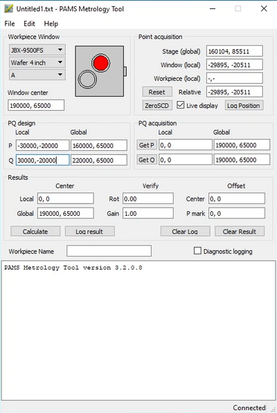
To get started using the prealigner, place the cassette front side down and the hook away from yourself. Log in on the computer and load PAMS Metrology Tool and PAMS Image Viewer. Verify that the coordinate output is correct by moving to the stage zero marker mounted on the bottom right of the prealigner, zero it on the coordinate display panel if it is more than a few µm off.
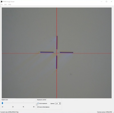
Move the stage to the center of your substrate, use the coordinates posted on the wall to find it easily. Find a feature that allows you to gauge the rotation, this can be a long straight line or two features that have the same Y-coordinate. Minimize the rotation by either rotating the slot using the set screws (not all cassettes have this) or by removing the substrate cover and rotate the substrate inside the slot. In the example below we have a cross (the P mark) which is obviously rotated relative to the red cross hair and the substrate should be rotated counter clockwise to compensate. Rotation should be so low that the Y-coordinate difference between the P and Q marks is less than 500 µm.
 |
|
|
Prealignment using the PAMS Metrology Tool and PAMS Microscope view. | |
Once the substrate rotation is fine it is time to find the actual alignment marks (P and Q marks). In the Metrology tool choose “JBX-9500FS” on the “Workpiece Window” dropdown and choose the substrate size and slot ID of your substrate. Enter the design coordinates of the P and Q marks in the “PQ design Local” fields.
Now find your P mark, align it to the red cross hair at 8X digital zoom and click “Get P”. Click it a few times as the first time always inputs an incorrect coordinate. Move to your Q mark, align to the cross hair and click “Get Q” a few times. Now click “Calculate”. The software will now calculate the rotation and gain. Verify that rotation is better than ± 1° and that the Y-coordinate difference is less than 500 µm, if not you should rotate the slot as described above. Also verify that the gain is close to 1. The gain is the ratio of measured distance between P and Q marks versus the design distance, ideally it should be 1. Finally press “Log result” to produce a text output. Copy and paste the output into a text file and save it with your exposure files, for instance to your M-drive. The procedure must naturally be carried out for all substrates that need alignment exposure.
When you are done with the alignment station, please close the programs, log off the computer and turn the microscope illumination down. Alert a member of the loading team to have your prealigned substrates loaded to the auto stocker.
| Example of output from the PAMS Metrology Tool |
|---|
PAMS Metrology Tool version 3.2.0.8 JBX-9500FS Wafer 4 inch A <> Registration result recorded 09-maj-2023, 11:15 Global mark P: design (-30000,-20000), stage (160108, 85480) Global mark Q: design ( 30000,-20000), stage (220107, 85909) Material cc : offset ( 250, -695), stage (190250, 65695) Gain 1.00001 Rotation 0.41 degrees OFFSET( 108, -480) ;(P mark) end<> |
System calibration
Execution of an aligned exposure has the same initial calibration steps as an unaligned exposure, i.e. it has the following steps
- Select and restore the system to the chosen beam current profile (RESTOR)
- Execute a current measurement (CURRNT)
- Execute absorbed electron mark detection (INITAE)
- Execute backscatter electron mark detection (INITBE)
- Execute self calibration routine daily
- Verify drift is low (DRIFT)
- Map height profile of sample (HEIMAP)
After sample height verification follows a few aditional steps to verify the system can find the substrate alignment marks.
Auto Gain Correction - AGCRG
Alignment is done by scanning the beam over the alignment marks and recording the backscatter electron intensity. Thus, it is essential that the gain of the detector system is set to match the substrate material, the mark material and the beam current. The system can automatically optimize the gain of the backscatter detector through the AGCRG subprogram. Bear in mind, it is not always possible to get sufficient signal. Al alignment marks on a Si substrate will for instance basically never work since the atomic number and hence backscatter intensity of the two materials are almost the same.
 |
|
|
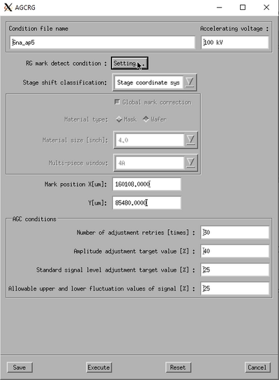
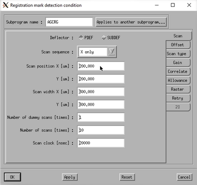
Setup of the AGCRG subprogram. | |
Choose the AGCRG subprogram from the calibration menu and edit the properties to set it up correctly. In order to optimise the gain it is naturally vital that the beam is actually scanning a mark. The easiest way to ensure this is to use the P mark stage coordinate from the prealigner output file. To do this, set the Stage shift classification to Stage coordinate system and enter the P mark stage coordinates from the prealigner in the Mark position fields. The AGC conditions can typically be left as they are.
Edit the scan conditions on the Settings button.
In the Scan pane one can set the Scan position and Scan width to suitable values for the mark in question. In general one should scan a cross at a position half way from the center and at least a width of 300 µm to be sure to hit it. In the Offset pane make sure the offsets are all set to zero. Click Ok and execute the scan.
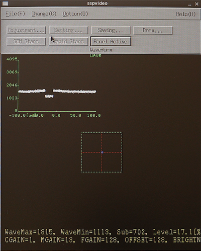
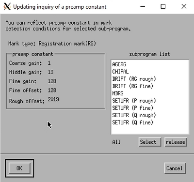
The system will now scan the mark position and attempt to optimise the detected backscatter signal in an iterative loop. After a successful scan the last scan result is displayed. It should show a distinct feature where the mark is detected. The aptly named Updating inquiry of a preamp constant window will also open. This shows the preamp constants along with a subprogram list that uses the backscatter detector and hence these constants. Copy the constants to all subprograms by clicking Select and OK. Now all necessary subprograms have the correct gain/preamp settings.
 |
|
|
Result of a successful gain optimisation. | |
Global alignment - SETWFR
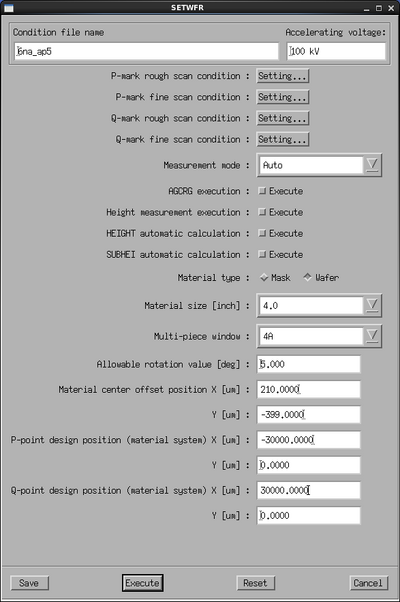
The next step is to verify that it is possible to detect the P and Q marks, this is done with the SETWFR subprogram. Select it and edit the parameters.
 |
 |
|
|
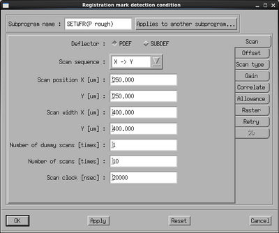
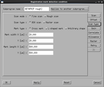
The SETWFR window and Settings scan condition windows. | ||
Set the Measurement mode to Auto. Make sure that Material type is set to Wafer. Set the Material size and Multi-piece window correctly to your exposure. In the Material center offset position fields enter the P mark offset as found from the prealigner. Enter the P and Q mark design coordinates in the last four fields. Based on the chosen window, the design coordinates and the prealigner offset, the system now knows where to look for the P mark.
Next, the scan parameters have to be set. There are four sets of scan parameters to set:
- P mark rough scan
- P mark fine scan
- Q mark rough scan
- Q mark fine scan
The rough scan conditions are used to scan over several 100 µm to find the mark while the fine scan conditions are used to accurately determine the center in as small a window as possible. Edit the P mark rough conditions by clicking its Setting button. Set the scan position x and y to about half the size of the mark, in this case 250 µm. Set the scan width in x and y to 400 µm to scan a large area with a high chance of finding the mark. If the contrast of the mark is not optimal the number of scans or the scan clock (beam dwell time) can be increased. Go to the Offset pane and make sure all offsets are set to zero. Go to the Scan type pane and set the mark width and mark length according to the mark, in this case 20 µm and 500 µm, respectively. The mark width is the most important as the system will only acknowledge a feature of the stated dimension to be the mark. With the condition setup, copy the settings to both the Q rough scan and the drift rough scan conditions using the Applies to another subprogram button. Close the window on OK.
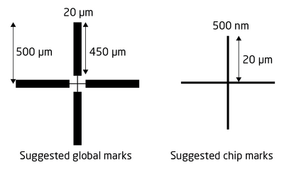
Also edit the fine scan conditions of the P mark. The windows are essentially identical, the only difference is the dimensions as we now want to scan a much smaller area in order to pinpoint the mark center with as high accuracy as possible. Ideally the mark should be similar to the one shown below with a wide part for the rough scan and a narrow part at the center for fine scan. In the fine scan define the scan position to be 20-30 µm from the center and set the width to 10 µm or less. The scan is made with 4000 datapoints along the scan axis, thus for a 10 µm wide scan the position resolution is 2.5 nm. The maximum resolution is 1 nm, thus if one defines a scan width less than 4 µm there will simply be less datapoints along the scan axis. Again, copy the settings to the Q mark fine condition and the drift fine scan condition via the Applies to another subprogram button.
| |
|
Alignment marks used in this example. | |
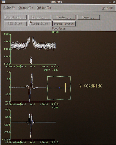
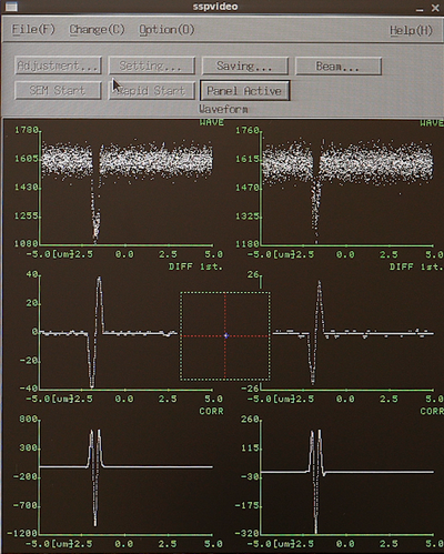
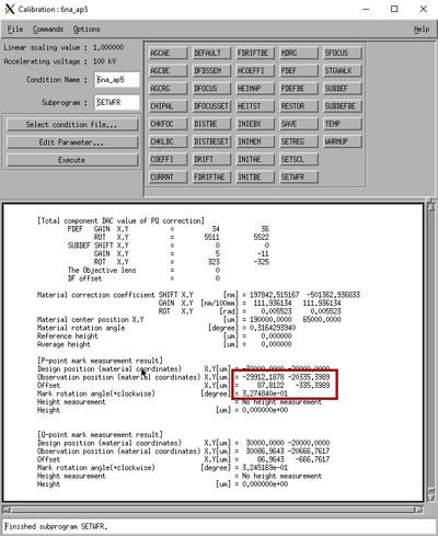
From the SETWFR window click Save and Execute. The mark scan will start with the P mark rough scan, if the mark is found it will continue to P mark fine scan, if successful the system will continue with Q mark rough scan and finally Q mark fine scan. Below is a few examples of an mark scan routine. In the left image the system has scanned the mark in the x-direction and found a nice feature, the yellow line indicates the system is currently scanning in y. Observe that in a y-axis scan the beam scans along the y-axis to determine the x-coordinate of the mark and vice versa. The center image shows a completed fine scan in a 10 µm window. The last image shows the data output after successfull mark detection. The important parameter is the P mark observation position offset. In this case the offset is (88,-335), this is entered in the SDF file OFFSET command to make sure the mark is easily found during job execution.
 |
 |
|
|
Examples of PQ mark detection scans. Left: P mark rough scan. Center: P mak fine scan. Right: Output in the Calib window. | ||
Chip alignment - CHIPAL
If the exposure uses chip alignment it should be setup and tested with the CHIPAL subprogram. Any chip with a scan mark can be used to test the chip alignment settings, one must of course know the center position of the chip as defined with the ARRAY command in the JDF.
 |
|
|
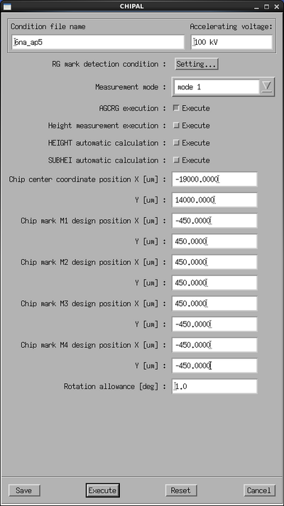
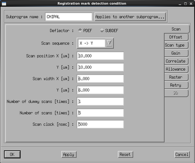
CHIPAL parameter window and CHIPAL scan conditions. | |
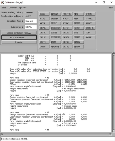
Select the CHIPAL subprogram and edit the parameters. In the Measurement mode choose Mode 1 or Mode 4 for one or four mark detection, respectively. Enter the chip center coordinates in the Chip center coordinate position (global coordinates). Enter the chip alignment marks (local chip coordinate system) in the Chip mark Mx design position fields. This will determine the position of the test scan. The scan parameters with the Settings button. In the settings window set the scan position close to the center of the mark, typically 10 µm. Make the scan width fairly small for best accuracy, just like for the rough scan the scan will consist of 4000 datapoints. Make sure the offsets are set to zero in the Offset pane and that the correct mark dimensions are set in the Scan type pane. Accept the parameters with OK and click Save and Execute in the CHIPAL window.
 |
|
|
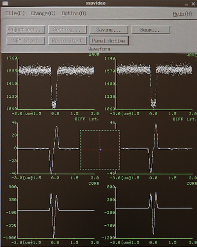
Chip mark scan result in the SSP window and the Calib window. | |
The chip mark is now scanned and the resulting backscatter signal can be seen in the SSP window. After successfull mark scan the result will also be shown in the Calib window.
Job execution
After successful execution of SETWFR and CHIPAL the condition file can now be saved and the exposure job can be executed, just as in the case of an unaligned exposure.
Alignment troubleshooting
Alignment on the JEOL system can be tricky, in this section we will briefly try and explain the cause and remedy for the most common problems encountered during the alignment process or job execution.
Nothing detected in P mark rough scan
Possible cause
- The gain settings are not correct.
- The scan width is not big enough, i.e. the scan does not hit the mark.
- Scan width is already 500 µm but still there is no signal.
Solutions
- If the gain settings are not correct they can be adjusted via the automatic gain correction program AGCRG as described in the procedure above.
- Increase scan width to 500 µm. There is cassette dependent offset between the prealigner stage coordinate and the actual system coordinate, increasing the scan width to 500 µm should however always overcome this offset.
- If the mark is made with a very thin line it can be hard to detect in a wide scan. The scan will consist of 4000 datapoints, if for instance the scan width is 500 µm the resolution of the scan is 125 nm. If the mark is only 1 µm wide it would show up in 8 points out of 4000 datapoints, that is not enough for the system to accept it as a feature.
Using the SEM for position verification
If marks can not be found it can be necessary to use the SEM mode to manually verify the stage coordinate of the mark. Using the SEM mode should be kept at a minimum as the SEM mode will expose the area you are looking at and, more importantly to the tool, it will evaporate resist off your sample and into the system. Thus SEM use should be kept at a minimum and SEM should not be used on resist covered areas at beam currents higher than 6 nA.
2D alignment option
In addition to alignment by beam scanning the JEOL 9500 system also has a 2D alignment feature. The working principle of this is that the system will take a SEM image of a specified location and compare the SEM image to a reference image. By comparison of these the system will determine an offset and use this for alignment.
Possible advantages of this is
- Alignment can be done using either the Secondary Electron or the Back Scatter detector or a combination of them
- Alignment might be possible to features with very low contrast
- Alignment can be done to an arbitrary shape
The following will illustrate how to set this up. It is a bit more complicated than regular beam scan alignment and knowledge of beam scan alignment is a prerequisite for understanding the following. Please contact us if you would like to try this alignment mode rather than trying on your own. For reference, the JEOL provided manual for 2D alignment can be found here: File:2D mark detecting 20171212.pdf
Reference images
During alignment the system will take SEM images and compare these to reference images of the alignment marks. These reference images can in principle be SEM images obtained from the system but it is simpler to use black and white drawings of the alignment marks. In this example we will use a cross as illustrated below.

|
|
Alignment mark used in this example. The mark is 1000 µm in both directions. |
The system must know the scale of the mark it is looking for, hence one must assign a physical dimension to the reference mark. The reference image must also be converted to a TIFF image. Both dimension assignment and conversion to TIFF is done with a command in a terminal window. In this example the actual mark is 1000 x 1000 µm and the input image is a PNG file called "PQRef1000mu.png". The command is:
ebimg setsize inputimage.png outputimage.tiff dimension
The dimension is given in nanometer. In the example the actual command is
ebimg setsize PQRef1000mu.png PQRef1000mu.tiff 1000000
This will generate a TIFF file with a scale of 1000 µm. Next, this must be converted with yet another command to a .ref.gz file. The command is
ebimg mkref inputimage.tiff outputimage.ref.gz
In our case it will be
ebimg mkref PQRef1000mu.tiff PQRef1000mu.ref.gz
After entering this command a window will open, showing the reference mark with a green cross indicating the center. For a symmetric mark this green cross will be in the center. It is possible to change the center point of the mark by moving the green mark with the mouse, this could be useful if an asymmetric mark is used. However, for a symmetric mark simply press "ESC" to close the window. This will generate the actual reference image file with the correct scaling. This file should be moved to
/home/eb0/jeoleb/prm/mark
SETWFR and CHIPAL setup
The alignment procedure is setup using the same subprograms as usual. The only difference is that we select a different scan type. Thus, in the "Scan Condition Settings" window, in the "Scan Type" pane, we select "Arbitrary shape" instead of the usual "Cross mark". This enables the "2D" pane of the settings window. In the "2D" pane we can now set a scan size, which should be similar to the feature size or slightly larger. With the "Reference" button we can select the reference image file previously generated. In this example we use a cross but as the "Arbitrary shape" scan type suggests, an arbitrary shape can be used.
 |

|
|
Settings of the "Scan type" and "2D" panes. | |
Finally, in the "Gain" pane we can setup the gain parameters. Notice that it is possible to switch between "BE" and "SE", i.e. backscattered electrons and secondary electrons. Depending on the layer stack and materials there can be a big difference in the contrast and this is the only way on the system to use secondary electrons for alignment.
It can be difficult to get these gain settings right. The best option is to move the stage to the mark location, turn on SEM mode, find working settings manually and copy these to the scan conditions using the "Applies to another subprogram..." feature.

|
|
Gain settings used for image scan. Unlike the usual "Cross mark" scan type, the "SE" detector is now available for alignment. |
Setup for CHIPAL scan conditions is exactly the same as for SETWFR and hence we will skip it here.
Execution
Execution is like usual by either running SETWFR or CHIPAL or the usual commands for automatic execution. During execution the system will make imagescans with the chosen detector and compare the resulting image with the reference file. If the match is accepted, the system will continue to the next mark. Below is the result of our example.
 |

|
|
Imagescans obtained during alignment. Rough alignment scan (left) is 1000 µm while fine scan (right) is 10 µm. The green cross indicates the center as determined by the system. | |

