Specific Process Knowledge/Etch/KOH Etch/ProcessInfo: Difference between revisions
| (16 intermediate revisions by one other user not shown) | |||
| Line 1: | Line 1: | ||
'''Feedback to this page''': '''[mailto:labadviser@danchip.dtu.dk?Subject=Feed%20back%20from%20page%20http://labadviser.danchip.dtu.dk/index.php/Specific_Process_Knowledge/Etch/KOH_Etch/ProcessInfo click here]''' | '''Feedback to this page''': '''[mailto:labadviser@danchip.dtu.dk?Subject=Feed%20back%20from%20page%20http://labadviser.danchip.dtu.dk/index.php/Specific_Process_Knowledge/Etch/KOH_Etch/ProcessInfo click here]''' | ||
'''Unless anything else is stated, everything on this page, text and pictures are made by DTU Nanolab.''' | |||
'''All links to Kemibrug (SDS) and Labmanager Including APV and QC requires login.''' | |||
==QC== | ==QC== | ||
===Quality Control (QC) for the KOH Si etching baths.=== | ===Quality Control (QC) for the KOH Si etching baths.=== | ||
'''All links in the table below reguire login to labmanager''' | |||
{| border="1" cellspacing="2" cellpadding="2" colspan="3" | {| border="1" cellspacing="2" cellpadding="2" colspan="3" | ||
|bgcolor="#98FB98" |'''Quality Control (QC) for Si Etch 01, and Si Etch 02''' | |bgcolor="#98FB98" |'''Quality Control (QC) for Si Etch 01, and Si Etch 02''' | ||
| Line 11: | Line 16: | ||
*[http://labmanager.dtu.dk/d4Show.php?id=5476&mach=407 The QC procedure for Si Etch: 03]<br> | *[http://labmanager.dtu.dk/d4Show.php?id=5476&mach=407 The QC procedure for Si Etch: 03]<br> | ||
{| {{table}} | {| {{table}} | ||
| align="center" | | | align="center" | | ||
{| border="1" cellspacing="1" cellpadding="2" align="center" style="width:200px" | {| border="1" cellspacing="1" cellpadding="2" align="center" style="width:200px" | ||
| Line 25: | Line 30: | ||
|Time | |Time | ||
|90 min | |90 min | ||
|- | |- | ||
|Substrate | |Substrate | ||
| Line 77: | Line 79: | ||
<math>X=\frac{(Y\cdot 1000g)}{(1.509g/ml\cdot(0.5-Y))}</math> | <math>X=\frac{(Y\cdot 1000g)}{(1.509g/ml\cdot(0.5-Y))}</math> | ||
| Line 96: | Line 99: | ||
Due to the almost inert (111)-planes it is possible by KOH etching to realize high aspect ratio structures in sigle crytalline silicon using the (111)-planes as sidewalls. In Si(100) these sidewalls are inclined - 54.7<sup>o</sup> with respect to the (100) surface - whereas in Si(110) the sidewalls are vertical (see figures below). | Due to the almost inert (111)-planes it is possible by KOH etching to realize high aspect ratio structures in sigle crytalline silicon using the (111)-planes as sidewalls. In Si(100) these sidewalls are inclined - 54.7<sup>o</sup> with respect to the (100) surface - whereas in Si(110) the sidewalls are vertical (see figures below). | ||
<gallery caption="Anisotropic wet silicon etch: dependency on crystal orientation" widths=" | <gallery caption="Anisotropic wet silicon etch: dependency on crystal orientation" widths="760px" heights="150px" perrow="1"> | ||
Image:KOH_Anisotropy.jpg|Etched profile when etching Si(100). | |||
Image:KOH_Anisotropy(110).jpg|Etched profile when etching Si(110). | Image:KOH-etch.JPG|Etched profile when etching Si(100) and when etching Si(110) respectively | ||
<!-- Image:KOH_Anisotropy.jpg|Etched profile when etching Si(100).--> | |||
<!-- Image:KOH_Anisotropy(110).jpg|Etched profile when etching Si(110).--> | |||
</gallery> | </gallery> | ||
<br clear="all"/> | <br clear="all"/> | ||
For Si(100), the relation between the width of the bottom of the etched groove (W<sub>b</sub>) and the width of the opening (W<sub>o</sub>) at the wafer surface in a groove etched to the depth | For Si(100), the relation between the width of the bottom of the etched groove (W<sub>b</sub>) and the width of the opening (W<sub>o</sub>) at the wafer surface in a groove etched to the depth d is given by: | ||
<math>W_b = W_o - 2d cot(54.7^o) = W_o - \sqrt{2} d</math> | |||
| Line 112: | Line 119: | ||
===Definition of <110> alignment structures=== | ===Definition of <110> alignment structures=== | ||
The etch rate dependence on the crystallographic planes can be used to determine the <110> crystal directions with high precision (better than +/- 0.05 <sup>o</sup>). A fast method for doing this, using the symmetric under-cutting behavior around but not at the <110>-directions, was described by Vangbo and Bäcklund | The etch rate dependence on the crystallographic planes can be used to determine the <110> crystal directions with high precision (better than +/- 0.05 <sup>o</sup>). A fast method for doing this, using the symmetric under-cutting behavior around but not at the <110>-directions, was described by [https://iopscience.iop.org/article/10.1088/0960-1317/6/2/011/meta Mattias Vangbo and Ylva Bäcklund 1996 J. Micromech. Microeng. '''6''', 279-284]. High-precision control of the <110>-direction during alignment can be necessary in order to control the dimensions of KOH-etched structures (e.g. precise control of V-groove dimensions). | ||
<br clear="all" /> | <br clear="all" /> | ||
===Etch rates: Empirical formula (Seidl et al)=== | <!-- ===Etch rates: Empirical formula (Seidl et al)=== | ||
The following empirical formula can be used for concentrations in the range of 10-60 wt%: | The following empirical formula can be used for concentrations in the range of 10-60 wt%: | ||
| Line 124: | Line 131: | ||
where k<sub>0</sub> = 2480 µm/hr (mol/l)<sup>-4.25</sup>, E<sub>a</sub> = 0.595 eV for Si(100) | where k<sub>0</sub> = 2480 µm/hr (mol/l)<sup>-4.25</sup>, E<sub>a</sub> = 0.595 eV for Si(100) | ||
and k<sub>0</sub> = 4500 µm/hr (mol/l)<sup>-4.25</sup>, E<sub>a</sub> = 0.60 eV for Si(110) | and k<sub>0</sub> = 4500 µm/hr (mol/l)<sup>-4.25</sup>, E<sub>a</sub> = 0.60 eV for Si(110) --> | ||
Latest revision as of 11:46, 28 July 2025
Feedback to this page: click here
Unless anything else is stated, everything on this page, text and pictures are made by DTU Nanolab.
All links to Kemibrug (SDS) and Labmanager Including APV and QC requires login.
QC
Quality Control (QC) for the KOH Si etching baths.
All links in the table below reguire login to labmanager
| Quality Control (QC) for Si Etch 01, and Si Etch 02 | ||||||||||||||||||||||||||||||
|
Mixing KOH
Nanolabs standard solution in the KOH baths has a concentration of 28 wt% and is mixed of 1 liter of a premade 50wt% KOH solution to 1.2 l of water.
If you use the 50wt% premade KOH solution you can calculate the amount of solution X you need to add 1 liter of water to achieve a concentration of Y wt% by:
where 1.509 g/ml is the density of a 50wt% solution KOH at 20 °C.
So for a 10 wt% solution you will need 165 ml of KOH (50wt%) to 1 l of water.
Backside protection
It is possible to protect the backside of the wafer against the KOH etch using special wafer holder.
Nanolab has backside protection holders for the two baths KOH 2 and KOH 3 for 4” wafer, and it is possible to mount two wafers in one holder. The material is PEEK, which is suitable for nearly all etchants and you will find the holders by the KOH baths. The recommended space from the wafer edge to your pattern is 7 mm. The thickness of the wafer would typically be 350 μm and the wafer would typically be polished on both sides, however with the right gasket (contact wet chemistry) the holders can accommodate 500-525 μm wafers. In order to avoid differences in pressure between the backside of the wafer and the surrounding environment, the venting tubes should be filled with water. The holder is clamped around the wafers by screws, if these screws are tightened too much or too little, it will affect the etching result. For the KOH 2 bath we have another type of holder which is clamped around the wafer with clamps (it cannot be adjusted to another wafer thickness). See more specific details about the screwed holders here, the holders we have at Nanolab is the Tandem4 type.
Theory
Definition of structures
Due to the almost inert (111)-planes it is possible by KOH etching to realize high aspect ratio structures in sigle crytalline silicon using the (111)-planes as sidewalls. In Si(100) these sidewalls are inclined - 54.7o with respect to the (100) surface - whereas in Si(110) the sidewalls are vertical (see figures below).
- Anisotropic wet silicon etch: dependency on crystal orientation
-
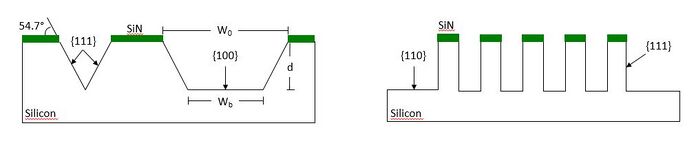 Etched profile when etching Si(100) and when etching Si(110) respectively

For Si(100), the relation between the width of the bottom of the etched groove (Wb) and the width of the opening (Wo) at the wafer surface in a groove etched to the depth d is given by:
Definition of <110> alignment structures
The etch rate dependence on the crystallographic planes can be used to determine the <110> crystal directions with high precision (better than +/- 0.05 o). A fast method for doing this, using the symmetric under-cutting behavior around but not at the <110>-directions, was described by Mattias Vangbo and Ylva Bäcklund 1996 J. Micromech. Microeng. 6, 279-284. High-precision control of the <110>-direction during alignment can be necessary in order to control the dimensions of KOH-etched structures (e.g. precise control of V-groove dimensions).