LabAdviser/314/Microscopy 314-307/SEM/AFEG: Difference between revisions
Appearance
No edit summary |
mNo edit summary |
||
| (5 intermediate revisions by the same user not shown) | |||
| Line 1: | Line 1: | ||
'''Feedback to this page''': '''[mailto:labadviser@nanolab.dtu.dk?Subject=Feed%20back%20from%20page%20http://labadviser.nanolab.dtu.dk/index.php/LabAdviser/314/Microscopy_314-307/SEM/AFEG click here]''' | |||
''This section is written by DTU Nanolab internal if nothing else is stated.'' | |||
[[index.php?title=Category:314]] | |||
[[index.php?title=Category:314-Microscopy]] | |||
__FORCETOC__ | __FORCETOC__ | ||
=AFEG 250 Analytical ESEM (FEI Quanta FEG 250) = | =AFEG 250 Analytical ESEM (FEI Quanta FEG 250) = | ||
| Line 94: | Line 99: | ||
|- | |- | ||
|} | |} | ||
Latest revision as of 11:15, 9 September 2025
Feedback to this page: click here
This section is written by DTU Nanolab internal if nothing else is stated. index.php?title=Category:314 index.php?title=Category:314-Microscopy
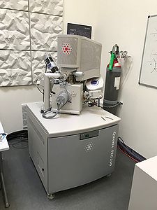
AFEG 250 Analytical ESEM (FEI Quanta FEG 250)

The AFEG is an FEI Quanta FEG 250(Field Emission Gun) scanning electron microscope with a spatial resolution of 2 nm for the ETD detector in high vacuum at 30 keV. The microscope can operate in high vacuum and low vacuum modes at room temperature. Our AFEG is fitted with EDS and WDS detectors, which allows for analytical measurements in all the operation modes.
Process information
- Electron source
- Field emission gun
- Accelerating voltage
- 500 V- 30 kV
- Resolution
- 2 nm at 30 kV (SE)
- Imaging detectors
- Everhart-Thornley (SE/BSE)
- Solid State BSE
- Large Field (LVD)
- Gaseous SE (GSED)
- Gaseous BSE
- Gaseous Analytical (GAD)
- STEM
- vCD
- Imaging modes
High and low vacuum
- Analytical capabilities
- Energy dispersive X-rays (Oxford Instruments 50 mm2 X-Max silicon drift detector, MnKα resolution at 124 eV)
- Wavelength Dispersive Spectrosopy
| Equipment | AFEG FEI Quanta FEG 250 | |
|---|---|---|
| Purpose | Vizualization and Microanalysis |
|
| Performance | Resolution | The resolution of AFEG depends on the sample and the operation mode! |
| ||
| Instrument specifics | Detectors |
|
| Electron source |
| |
| Stage (room temperature) |
| |
| WDS |
| |
| EDS |
| |
| Operating pressures |
| |
| Samples | Sample sizes |
|
| Allowed materials |
| |
