Specific Process Knowledge/Back-end processing/Die Bonder: Difference between revisions
Appearance
No edit summary |
|||
| (5 intermediate revisions by 4 users not shown) | |||
| Line 2: | Line 2: | ||
<!-- Replace "http://labadviser.nanolab.dtu.dk/..." with the link to the Labadviser page--> | <!-- Replace "http://labadviser.nanolab.dtu.dk/..." with the link to the Labadviser page--> | ||
[[image:Die-bonder_Cammax_EDB-80.jpg|200x200px|thumb|The Die-bonder Cammax EDB-80 is placed in | [[image:Die-bonder_Cammax_EDB-80.jpg|200x200px|thumb|The Die-bonder Cammax EDB-80 is placed in the Packlab in building 347, 1st floor.]] | ||
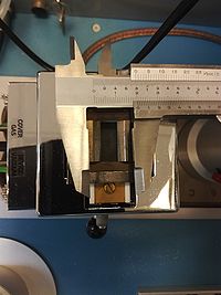
[[image:DieBonderHeatingChuck.jpg|200x300px|thumb|Heating Chuck on the Die-bonder]] | [[image:DieBonderHeatingChuck.jpg|200x300px|thumb|Heating Chuck on the Die-bonder]] | ||
== Die bonder (eutectic metal soldering) == | == Die bonder (eutectic metal soldering) == | ||
The Cammax EDB80 Die bonder is for placing and soldering dies onto a package or substrate. | The Cammax EDB80 Die bonder is for placing and soldering dies onto a package or substrate. | ||
''The Cammax EDB80 Die bonder is currently (only temporary) taken out of service during the PolyFabLab construction.'' | |||
The bonder has a graphite heater element enabling fast heating to the melting point of the solder. To prevent oxidation of the solder and bonding surfaces it is possible to have a gas flow of formier gas (4-10% H2 in N2) over the sample. The machine also has a pick-up tool enabling accurate placement of the sample onto a carrier. | The bonder has a graphite heater element enabling fast heating to the melting point of the solder. To prevent oxidation of the solder and bonding surfaces it is possible to have a gas flow of formier gas (4-10% H2 in N2) over the sample. The machine also has a pick-up tool enabling accurate placement of the sample onto a carrier. | ||
| Line 18: | Line 20: | ||
== Process information == | == Process information == | ||
none | |||
<br/> | <br/> | ||
<br/> | <br/> | ||
| Line 27: | Line 29: | ||
<br/> | <br/> | ||
<br/> | <br/> | ||
==Equipment performance and process related parameters== | ==Equipment performance and process related parameters== | ||
| Line 48: | Line 36: | ||
!colspan="2" border="none" style="background:silver; color:black;" align="center"|Equipment | !colspan="2" border="none" style="background:silver; color:black;" align="center"|Equipment | ||
|style="background:WhiteSmoke; color:black"|<b>Die bonder</b> | |style="background:WhiteSmoke; color:black"|<b>Die bonder</b> | ||
|- | |- | ||
!style="background:silver; color:black;" align="center" width="60"|Purpose | !style="background:silver; color:black;" align="center" width="60"|Purpose | ||
| Line 55: | Line 42: | ||
*Fine placement of dies | *Fine placement of dies | ||
*Eutectic metal soldering | *Eutectic metal soldering | ||
|- | |- | ||
!style="background:silver; color:black;" align="center" width="60"|Performance | !style="background:silver; color:black;" align="center" width="60"|Performance | ||
| Line 64: | Line 48: | ||
*Low thermal resistance | *Low thermal resistance | ||
*Always conducting | *Always conducting | ||
|- | |- | ||
!style="background:silver; color:black" align="center" valign="center" rowspan="3"|Substrates | !style="background:silver; color:black" align="center" valign="center" rowspan="3"|Substrates | ||
| Line 74: | Line 54: | ||
*Should be able to withstand the soldering temperature | *Should be able to withstand the soldering temperature | ||
*Typical materials are: Alumina (Al2O3), AluminumNitride (AlN) | *Typical materials are: Alumina (Al2O3), AluminumNitride (AlN) | ||
|- | |- | ||
|} | |} | ||
<br clear="all" /> | <br clear="all" /> | ||
Latest revision as of 16:52, 3 July 2025
Feedback to this page: click here


Die bonder (eutectic metal soldering)
The Cammax EDB80 Die bonder is for placing and soldering dies onto a package or substrate.
The Cammax EDB80 Die bonder is currently (only temporary) taken out of service during the PolyFabLab construction.
The bonder has a graphite heater element enabling fast heating to the melting point of the solder. To prevent oxidation of the solder and bonding surfaces it is possible to have a gas flow of formier gas (4-10% H2 in N2) over the sample. The machine also has a pick-up tool enabling accurate placement of the sample onto a carrier.
The user manuals, user APVs, technical information and contact information can be found in LabManager:
Process information
none
| Equipment | Die bonder | |
|---|---|---|
| Purpose |
| |
| Performance |
| |
| Substrates | Allowed materials |
|
