Specific Process Knowledge/Etch/DRIE-Pegasus/Etch silicon nanostructures: Difference between revisions
No edit summary |
mNo edit summary |
||
| (13 intermediate revisions by 3 users not shown) | |||
| Line 1: | Line 1: | ||
'''Feedback to this page''': '''[mailto:labadviser@ | '''Feedback to this page''': '''[mailto:labadviser@nanolab.dtu.dk?Subject=Feed%20back%20from%20page%20http://labadviser.nanolab.dtu.dk/index.php/Specific_Process_Knowledge/Etch/DRIE-Pegasus/Etch_silicon_nanostructures click here]''' | ||
<!--Checked for updates on 24/8-2021. ok/ jmli--> | |||
<!--Checked for updates on 4/4-2025 - ok/jmli --> | |||
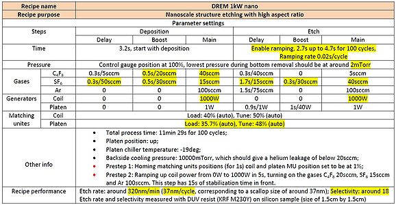
Based on the so called DREM process, there are two recipes on DRIE-Pegasus 1 which are suitable for etching silicon nanostructures. The recipes are called '''DREM 1kW nano''' and '''DREM 0.5kW nano'''. In '''DREM 1kW nano''' a higher coil power and larger gas flow rates are applied, making it suitable for etching high aspect ratio nanostructures (AR around 25 can be achieved depending on the patterns and resist used). In '''DREM 0.5kW nano''' both the coil power and gas flow rates are reduced, thus the scallop size can be reduced remarkably down to 16nm, giving a smooth sidewall on the nanostructures, while the aspect ratio can be limited. The recipes can be chosen based on the purpose of users, and the parameters are listed as below (different parameters are highlighted): | Based on the so called DREM process, there are two recipes on DRIE-Pegasus 1 which are suitable for etching silicon nanostructures. The recipes are called '''DREM 1kW nano''' and '''DREM 0.5kW nano'''. In '''DREM 1kW nano''' a higher coil power and larger gas flow rates are applied, making it suitable for etching high aspect ratio nanostructures (AR around 25 can be achieved depending on the patterns and resist used). In '''DREM 0.5kW nano''' both the coil power and gas flow rates are reduced, thus the scallop size can be reduced remarkably down to 16nm, giving a smooth sidewall on the nanostructures, while the aspect ratio can be limited. The recipes can be chosen based on the purpose of users, and the parameters are listed as below (different parameters are highlighted): | ||
{| | |||
| [[Image:DREM1.jpg |thumb|x300px|Parameter settings DREM 1kW nano]] | |||
| [[Image:DREM2.jpg |thumb|x300px|Parameter settings DREM 0.5kW nano]] | |||
|} | |||
Below are some etched silicon nanostructures with the recipe '''DREM 1kW nano''' | Below are some etched silicon nanostructures with the recipe '''DREM 1kW nano''' | ||
{| | |||
| [[Image:DREM1pic1.jpg |thumb|x300px|200nm trenches etched with 125 cycles (cross section view)]] | |||
| [[Image:DREM1pic2.jpg |thumb|x300px|200nm pillars etched with 100 cycles (cross section view)]] | |||
|- | |||
| [[Image:DREM1pic3.jpg |thumb|x300px|200nm pillars etched with 100 cycles (tilted view)]] | |||
| [[Image:DREM1pic4.jpg |thumb|x300px|Zoom in on top of 200nm pillars, showing the scallops (tilted view)]] | |||
|} | |||
Below are some etched silicon nanostructures with the recipe '''DREM 0.5kW nano''' | Below are some etched silicon nanostructures with the recipe '''DREM 0.5kW nano''' | ||
{| | |||
| [[Image:DREM2pic1.jpg |thumb|x300px|200nm trenches etched with 100 cycles (cross section view), a smooth sidewall can be seen with less scallop induced roughness]] | |||
| [[Image:DREM2pic2.jpg |thumb|x300px|200nm pillars etched with 100 cycles (cross section view)]] | |||
|- | |||
| [[Image:DREM2pic3.jpg |thumb|x300px|200nm pillars etched with 100 cycles (tilted view)]] | |||
| [[Image:DREM2pic4.jpg |thumb|x300px|Pillars etched with 100 cycles, patterns defined with EBL and ZEP resist, smallest dimesion of 100nm (tilted view)]] | |||
|} | |||
Extra caution is required for modification of recipe parameters, it is recommended to monitor the picoscope signals during the process, the process should be aborted manually if a high reflective power is observed either from coil or platen generators, thus hardware damage can be avoied. For more details, please contact Henri Jansen (henrija@dtu.dk) or Bingdong Chang (bincha@dtu.dk) | |||
Latest revision as of 08:27, 3 June 2025
Feedback to this page: click here
Based on the so called DREM process, there are two recipes on DRIE-Pegasus 1 which are suitable for etching silicon nanostructures. The recipes are called DREM 1kW nano and DREM 0.5kW nano. In DREM 1kW nano a higher coil power and larger gas flow rates are applied, making it suitable for etching high aspect ratio nanostructures (AR around 25 can be achieved depending on the patterns and resist used). In DREM 0.5kW nano both the coil power and gas flow rates are reduced, thus the scallop size can be reduced remarkably down to 16nm, giving a smooth sidewall on the nanostructures, while the aspect ratio can be limited. The recipes can be chosen based on the purpose of users, and the parameters are listed as below (different parameters are highlighted):
 |
 |
Below are some etched silicon nanostructures with the recipe DREM 1kW nano
Below are some etched silicon nanostructures with the recipe DREM 0.5kW nano
Extra caution is required for modification of recipe parameters, it is recommended to monitor the picoscope signals during the process, the process should be aborted manually if a high reflective power is observed either from coil or platen generators, thus hardware damage can be avoied. For more details, please contact Henri Jansen (henrija@dtu.dk) or Bingdong Chang (bincha@dtu.dk)


