Specific Process Knowledge/Thin film deposition/Physimeca: Difference between revisions
No edit summary |
|||
| (6 intermediate revisions by 3 users not shown) | |||
| Line 1: | Line 1: | ||
'''Feedback to this page''': '''[mailto:labadviser@danchip.dtu.dk?Subject=Feed%20back%20from%20page%20http://labadviser.danchip.dtu.dk/index.php/Specific_Process_Knowledge/Thin_film_deposition/Physimeca click here]''' | '''Feedback to this page''': '''[mailto:labadviser@danchip.dtu.dk?Subject=Feed%20back%20from%20page%20http://labadviser.danchip.dtu.dk/index.php/Specific_Process_Knowledge/Thin_film_deposition/Physimeca click here]''' | ||
<i> Unless otherwise stated, this page is written by <b>DTU Nanolab internal</b></i> | |||
[[Category: Equipment|Thin film Physimeca]] | [[Category: Equipment|Thin film Physimeca]] | ||
[[Category: Thin Film Deposition|Physimeca]] | [[Category: Thin Film Deposition|Physimeca]] | ||
== Physimeca == | == Physimeca - <span style="color:Red"> This tool has been decommissioned</span>== | ||
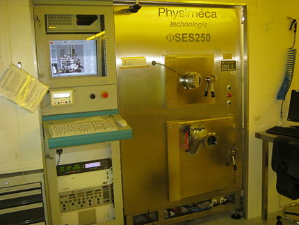
[[image:Physimeca.jpg|430x430px|right|thumb|The Physicmeca, | [[image:Physimeca.jpg|430x430px|right|thumb|The Physicmeca, Located in cleanroom B-1.]] | ||
Physimeca is a system for deposition of metals through electron-beam evaporation | Physimeca is a system for deposition of metals through electron-beam evaporation. | ||
Wafers are loaded into the system through the load lock and transferred into the deposition chamber. Physimeca allows you to deposit metals on samples | Wafers are loaded into the system through the load lock and transferred into the deposition chamber. Physimeca allows you to deposit metals on samples up to 4 inch wafer. There are three different sample holders, one for chips (arbitrary size), one for 2" wafers and one for 4" wafers. The sample holder can be tilted during deposition, but is normally kept in a horizontal orientation. | ||
Six different metals are present at each time in the Physimeca. The metal combination is changed if needed. A list of currently allowed metals is included in the table below; contact the ThinFilm team ( | Six different metals are present at each time in the Physimeca. The metal combination is changed if needed. A list of currently allowed metals is included in the table below; contact the ThinFilm team (Metal@nanolab.dtu.dk) if you have wishes for other metals. | ||
| Line 22: | Line 24: | ||
<br clear="all" /> | <br clear="all" /> | ||
==Equipment performance and process related parameters Physimeca== | ==Equipment performance and process related parameters Physimeca== | ||
| Line 36: | Line 37: | ||
|style="background:LightGrey; color:black"|Film thickness||style="background:WhiteSmoke; color:black"| | |style="background:LightGrey; color:black"|Film thickness||style="background:WhiteSmoke; color:black"| | ||
*10 Å - 5000 Å* | *10 Å - 5000 Å* | ||
|- | |- | ||
|style="background:LightGrey; color:black"|Available metals and deposition rates (Å/s) | |style="background:LightGrey; color:black"|Available metals and deposition rates (Å/s) | ||
| Line 49: | Line 50: | ||
*Silver (Ag) | *Silver (Ag) | ||
|- | |- | ||
!style="background:silver; color:black" align="left" valign="top" rowspan=" | !style="background:silver; color:black" align="left" valign="top" rowspan="3"|Process parameter range | ||
|style="background:LightGrey; color:black"|Process Temperature | |style="background:LightGrey; color:black"|Process Temperature | ||
|style="background:WhiteSmoke; color:black"| | |style="background:WhiteSmoke; color:black"| | ||
| Line 57: | Line 58: | ||
|style="background:WhiteSmoke; color:black"| | |style="background:WhiteSmoke; color:black"| | ||
* 2x10<sup>-6</sup> mbar | * 2x10<sup>-6</sup> mbar | ||
|- | |||
|style="background:LightGrey; color:black"|Distance between e-beam and substrate | |||
|style="background:WhiteSmoke; color:black"| | |||
* 46 cm | |||
|- | |- | ||
!style="background:silver; color:black" align="left" valign="top" rowspan="3"|Substrates | !style="background:silver; color:black" align="left" valign="top" rowspan="3"|Substrates | ||
|style="background:LightGrey; color:black"| | |style="background:LightGrey; color:black"|Sample size | ||
|style="background:WhiteSmoke; color:black"| | |style="background:WhiteSmoke; color:black"| | ||
*2 or 4" wafers | *one 2" or 4" wafers | ||
*Or several smaller pieces | *Or several smaller pieces | ||
| Line 80: | Line 85: | ||
|} | |} | ||
'''*''' ''For thicknesses above 2000 Å special permission is required (contact thinfilm@ | '''*''' ''For thicknesses above 2000 Å special permission is required (contact thinfilm@nanolab.dtu.dk).'' | ||
== [[/Physimeca_calibration|Calibration of Physimeca]] '' - for experienced users only'' == | == [[/Physimeca_calibration|Calibration of Physimeca]] '' - for experienced users only'' == | ||
Latest revision as of 09:45, 6 June 2023
Feedback to this page: click here
Unless otherwise stated, this page is written by DTU Nanolab internal
Physimeca - This tool has been decommissioned

Physimeca is a system for deposition of metals through electron-beam evaporation.
Wafers are loaded into the system through the load lock and transferred into the deposition chamber. Physimeca allows you to deposit metals on samples up to 4 inch wafer. There are three different sample holders, one for chips (arbitrary size), one for 2" wafers and one for 4" wafers. The sample holder can be tilted during deposition, but is normally kept in a horizontal orientation.
Six different metals are present at each time in the Physimeca. The metal combination is changed if needed. A list of currently allowed metals is included in the table below; contact the ThinFilm team (Metal@nanolab.dtu.dk) if you have wishes for other metals.
The user manual and contact information can be found in LabManager:
| Purpose | Deposition of metals |
|
|---|---|---|
| Performance | Film thickness |
|
| Available metals and deposition rates (Å/s) |
| |
| Process parameter range | Process Temperature |
|
| Process pressure |
| |
| Distance between e-beam and substrate |
| |
| Substrates | Sample size |
|
| Substrate material allowed |
| |
| Materials allowed on the substrate |
|
* For thicknesses above 2000 Å special permission is required (contact thinfilm@nanolab.dtu.dk).
