LabAdviser/Technology Research/Fabrication of Hyperbolic Metamaterials using Atomic Layer Deposition: Difference between revisions
mNo edit summary |
|||
| (60 intermediate revisions by 3 users not shown) | |||
| Line 1: | Line 1: | ||
'''Feedback to this page''': '''[mailto:labadviser@ | '''Feedback to this page''': '''[mailto:labadviser@nanolab.dtu.dk?Subject=Feed%20back%20from%20page%20http://labadviser.nanolab.dtu.dk/index.php/LabAdviser/Technology_Research/Fabrication_of_Hyperbolic_Metamaterials_using_Atomic_Layer_Deposition click here]''' | ||
<i>This page is written by <b>Evgeniy Shkondin @DTU Nanolab</b> if nothing else is stated. <br> | |||
All images and photos on this page belongs to <b>DTU Nanolab</b> and <b>DTU Electro</b> (previous DTU Fotonik).<br> | |||
The fabrication and characterization described below were conducted in <b>2013-2016 by Evgeniy Shkondin, DTU Nanolab</b>.<br></i> | |||
=Fabrication of Hyperbolic Metamaterials using Atomic Layer Deposition= | =Fabrication of Hyperbolic Metamaterials using Atomic Layer Deposition= | ||
*'''Project type:''' Ph.d project | *'''Project type:''' Ph.d project | ||
*'''Project responsible:''' | *'''Project responsible: Evgeniy Shkondin <br> [[image:orcid_16x16.png|16x16px]]https://orcid.org/0000-0002-8347-1814''' | ||
*'''Supervisors:''' Andrei Lavrinenko, Flemming Jensen | *'''Supervisors:''' Andrei Lavrinenko, Flemming Jensen | ||
*'''Partners involved:''' DTU Fotonik, DTU Danchip | *'''Partners involved:''' DTU Fotonik, DTU Nanolab (former DTU Danchip) | ||
*'''Full Thesis:''' https://orbit.dtu.dk/en/publications/fabrication-of-hyperbolic-metamaterials-using-atomic-layer-deposi | |||
==Project Description== | ==Project Description== | ||
[[image: | [[image:HMM_implementation_topology.png|600px|thumb|Figur 1. Schematics of (a) a multilayer and (b) a nanowire hyperbolic metamaterial.]] | ||
This project deals with the technological development, design, and fabrication of hyperbolic metamaterials (HMMs) - one of the most unusual classes of artificial electromagnetic subwavelength structures. Electrodynamically, HMMs are described by a dielectric permittivity tensor " with components of opposite signs (e.g. <math>\varepsilon_{x}=\varepsilon_{y}<0, \varepsilon_{z}>0</math> ). HMMs possess unusually high wavevector, the optical density of states, and anisotropy, leading to a wide variety of potential applications such as broadband enhancement in the spontaneous emission for a single photon source, subwavelength imaging, sensing, thermal engineering, and steering of optical signals. HMMs have a potential to be a robust and versatile multi-functional platform for nanophotonics in the broad range of operating wavelengths from visible to THz regions and even at microwave region. Despite the proposed architecture of hyperbolic medium, which geometry includes simple metal/dielectric multilayers (Figure 1a) and metallic wires (Figure 1b) incorporated in dielectric host, the fabrication is still challenging, since ultrathin, continuous, pinhole free nanometer-scale coatings are desired.<br> | |||
The required high-quality | The required high-quality thin layers have been fabricated using atomic layer deposition (ALD). It is a relatively new, cyclic, self-limiting thin film deposition technology allowing thickness control on the atomic scale. As the deposition relies on a surface reaction, conformal pinhole free films can be deposited on various substrates with advanced topology. This method has been a central theme of the project and a core fabrication technique of plasmonic and dielectric metamaterial | ||
The | components.<br> | ||
The deposition characteristics of the simplest and most studied ALD processes, Al<sub>2</sub>O<sub>3</sub> and TiO<sub>2</sub> were studied as a starting point. Later, the growth and characterization of ZnO semiconductor and Cu metal have been explored.<br> | |||
The ability to reproducibly deposit conformal TiO<sub>2</sub> and Al<sub>2</sub>O<sub>3</sub> dielectric coatings have been implemented in the optical experiment where the effective medium approximation theory (EMA) was tested. Flat dielectric multilayers with strict thicknesses of either 10 or 20 nm of each individual layer, were deposited on Si substrates and characterized using x-ray photoelectron spectroscopy (XPS) and scanning electron microscopy (SEM).<br> | |||
The next milestone was a technology development where the ALD dielectric coatings could be placed as the individual, separate units in one or two-dimensional lattices (gratings or pillars). This was achieved by combining ALD, deep ultra-violet (UV) stepper lithography and advanced silicon deep reactive ion etching (DRIE) techniques. Three different high aspect ratio, freestanding Al<sub>2</sub>O<sub>3</sub>, and TiO<sub>2</sub> structures have been successfully manufactured: gratings, pillars, and poly-cylindrical | |||
arrays. The challenge of Si template fabrication using DRIE and isolation of the final structures using selective Si etch were addressed.<br> | |||
Fabrication of HMMs requires the implementation of plasmonic components and traditionally noble metals are used for such purposes due to their abundant free electrons in the conduction band. However, their large real and imaginary parts of the permittivity, especially in the infrared range, result in high loss and weak confinement to the surface. Additionally, the most implemented metals in plasmonics such as Au and Ag are difficult to pattern at nanoscale due to their limited chemistry, adhesion or oxidation issues. Therefore the implementation of alternative plasmonic materials suitable for certain wavelength range has been the focus of this work.<br> | |||
Transparent conductive oxides such as Al-doped ZnO (AZO) have attracted significant attention as alternative plasmonic materials, due to their low loss and metallic behavior in the near/mid-infrared range. One more advantage of AZO is the possibility of tuning the permittivity by design, by deciding the dopants or the ratio of different components, thus constituting an advantage over metals having fixed permittivity values. AZO was chosen since the Cu ALD showed up to be far less successful in terms of reproducibility and conformality requirements. AZO has been grown on different substrates in the temperature range 150 <sup>o</sup>C - 250 <sup>o</sup>C and optical, electrical and physical properties have been clarified.<br> | |||
Finally, metamaterials with two different geometries have been realized, AZO trenches and AZO pillars standing in a dielectric host (air or Si). Furthermore, it has been proposed that high aspect ratio grating structures with AZO lamellas in a silicon matrix function as a versatile platform supporting both surface and volume infrared waves. By selective etching of Si the performance of the whole structure | |||
can be reconfigured. In other words, a bi-slab HMM has been suggested, where the effective properties of the structure are controlled by the thickness of the top slab (etching depth).<br clear="all" /> | |||
<gallery caption="Fabricated metamaterials based on Al-doped ZnO (AZO). Measurements performed using Fourier Trasform Infrared Spectroscopy (FTIR)." widths="500px" heights="500px" perrow="4"> | |||
image:AZO_Air_trench_SEM.jpg| AZO trenches in air host. SEM image, bird-eye-view. | |||
image:AZO_Si_trench_SEM.jpg| AZO trenches in Si host. SEM image, bird-eye-view. | |||
image:pillars.jpg| AZO pillars. SEM image, bird-eye-view. | |||
image:tubes.jpg| AZO tubes. SEM image, bird-eye-view. | |||
</gallery> | |||
<br clear="all" /> | |||
<gallery caption="Optical performance of fabricated metamaterials based on Al-doped ZnO (AZO)" widths="500px" heights="500px" perrow="4"> | |||
image:22.jpg| AZO trenches in air host. Enters hyperbolic regime for <math>\lambda>2.71 \mu m </math> | |||
image:11.jpg| AZO trenches in Si host. Enters hyperbolic regime for <math>\lambda>7.45 \mu m </math> | |||
image:33.jpg| AZO pillars in Si host. Metamaterial with high anisotropy in permittivity (not HMM). | |||
image:44.jpg| AZO pillars in Si host. Metamaterial with high anisotropy in permittivity (not HMM). | |||
</gallery> | |||
<br clear="all" /> | |||
==Publications in peer-review journals== | |||
===Midinfrared Surface Waves on a High Aspect Ratio Nanotrench Platform === | |||
O. Takayama, <u>E. Shkondin</u>, A. Bogdanov, M. E. Aryaee Panah, K. Golenicki, P. Dmitriev, T. Repän, R. Malureanu, P. Belov, F. Jensen & A. Lavrinenko. ACS Photonics, 2017, 4 (11), pp 2899–2907 [http://pubs.acs.org/doi/abs/10.1021/acsphotonics.7b00924 LINK] | |||
*[[/AZO_gratings|<strong>Procces flow</strong>]] | |||
===Large-Scale High Aspect Ratio Al-Doped ZnO Nanopillars Arrays as Anisotropic Metamaterials=== | |||
<u>E. Shkondin</u>, O. Takayama, M. E. Aryaee Panah, P. Liu, P. V. Larsen, M. D. Mar, F. Jensen. & A. Lavrinenko | |||
(2017). Optical Materials Express, 7(5), pp. 1606-1627 (2017) [https://www.osapublishing.org/ome/abstract.cfm?uri=ome-7-5-1606 LINK] | |||
*[[/AZO_pillars|<strong>Procces flow</strong>]] | |||
===Laguerre-Gauss Beam Generation in IR and UV by Subwavelength Surface-Relief Gratings=== | |||
L. Vertchenko, <u>E. Shkondin</u>, R. Malureanu, & C. Monken | |||
(2017). Optics Express, 25(6), pp. 5917-5926 (2017) [https://osapublishing.org/oe/abstract.cfm?uri=oe-25-6-5917 LINK] | |||
*[[/TiO2_Q_plates|<strong>Procces flow</strong>]] | |||
===Fabrication of High Aspect Ratio TiO<sub>2</sub> and Al<sub>2</sub>O<sub>3</sub> Nanogratings by Atomic Layer Deposition=== | |||
<u>E. Shkondin</u>, O. Takayama, J. Lindhard, P. V. Larsen, M. D. Mar, F. Jensen & A. Lavrinenko | |||
(2016). Journal of Vacuum Science and Technology A, 34, 031605 (2016) [http://scitation.aip.org/content/avs/journal/jvsta/34/3/10.1116/1.4947586 LINK] | |||
*[[/TIO_ALU_Gratings_Procces_flow|<strong>Procces flow</strong>]] | |||
===Experimental Demonstration of Effective Medium Approximation Breakdown in Deeply Subwavelength All-Dielectric Multilayers=== | ===Experimental Demonstration of Effective Medium Approximation Breakdown in Deeply Subwavelength All-Dielectric Multilayers=== | ||
S. Zhukovsky, A. Andryieuski, O. Takayama, <u>E. Shkondin</u>, R. Malureanu, F. Jensen, & A. Lavrinenko | |||
(2015) | (2015). Physical Review Letters, 115(17), 177402 [http://journals.aps.org/prl/abstract/10.1103/PhysRevLett.115.177402 LINK] | ||
*[[/EMT_Procces_flow|<strong>Procces flow</strong>]] | |||
<br> | |||
==Publications in proceedings== | |||
===Effective medium approximation for deeply subwavelength all-dielectric multilayers: when does it break down?=== | |||
A. Lavrinenko, S. Zhukovsky, A. Andryieuski, O. Takayama, <u>E. Shkondin</u>, R. Malureanu and F. Jensen <br> | |||
Proceedings of SPIE. Vol. 9883 SPIE - International Society for Optical Engineering, (2016) | |||
===Fabrication of deep-profile Al-doped ZnO one- and two-dimensional lattices as plasmonic elements=== | |||
F. Jensen, <u>E. Shkondin</u>, O. Takayama, P. V. Larsen, M. D. Mar, R. Malureanu, A. V. Lavrinenko <br> | |||
Proceedings of SPIE. Vol. 9921 SPIE - International Society for Optical Engineering, (2016) | |||
===Hyperbolic metamaterials with complex geometry=== | |||
A. V. Lavrinenko, A. Andryieuski, S. Zhukovsky, O. Takayama, <u>E. Skhondin</u>, M. E. Aryaee Panah, R. Malureanu, F. Jensen <br> | |||
META'16, The 6th International Conference on Metamaterials, Photonic Crystals and Plasmonics, Malaga, Spain, 2A23, Proceedings, p.471-472 (2016) | |||
===Surface waves on metal-dielectric metamaterials=== | |||
O. Takayama, <u>E. Shkondin</u>, M. E. Aryaee Panah, T. Repän, R. Malureanu, F. Jensen, A. V. Lavrinenko <br> | |||
Proceedings of 18th International Conference on Transparent Optical Networks. IEEE, (2016) | |||
===Surface waves on metamaterials interfaces=== | |||
O. Takayama, <u>E. Shkondin</u>, M. E. Aryaee Panah, T. Repän, R. Malureanu, F. Jensen, A. V. Lavrinenko <br> | |||
Proceedings of 10th International Congress on Advanced Electromagnetic Materials in Microwaves and Optics.(2016) | |||
===Ultra-thin metal and dielectric layers for nanophotonic applications=== | |||
<u>E. Shkondin</u>, L. Leandro, R. Malureanu, F. Jensen, N. Rozlosnik, A. V. Lavrinenko <br> | |||
Proceedings of ICTON, IEEE, 7193380. (2015) | |||
==Conferences and workshops== | |||
===Conductive oxides trench structures as hyperbolic metamaterials in mid-infrared range=== | |||
O. Takayama, <u>E. Shkondin</u>, M. E. A. Panah, T. Reän, R. Malureanu, F. Jensen, A. V. Lavrinenko <br> | |||
2016. Abstract from 14th International Conference of Near-Field Optics, Nanophotonics and Related Techniques, Hamamatsu, Japan | |||
===Fabrication of hollow coaxial ZnAl<sub>2</sub>O<sub>4</sub> high aspect ratio freestanding nanopillars based on the Kirkendall effect=== | |||
<u>E. Shkondin</u>, F. Jensen, A. V. Lavrinenko <br> | |||
2016. Abstract from 42nd Micro and Nano Engineering 2016, Vienna, Austria | |||
===Fabrication of Al-doped ZnO high aspect ratio nanowires and trenches as active components in mid-infrared plasmonics=== | |||
<u>E. Shkondin</u>, O. Takayama, P. V. Larsen, M. D. Mar, F. Jensen, A. V. Lavrinenko <br> | |||
2016. Abstract from 16th Atomic Layer Deposition Conference, Dublin, Ireland. | |||
===TiO<sub>2</sub> and Al<sub>2</sub>O<sub>3</sub> ALD grown multilayers for subwavelength photonics=== | |||
<u>E. Shkondin</u>, F. Jensen, A. V. Lavrinenko, M. D. Mar, P. V. Larsen, R. Malureanu, S. Zhukovsky, A. Andryieuski, O. Takayama <br> | |||
2015. DTU's Sustain Conference 2015, Technical University of Denmark, Kgs. Lyngby, Denmark (2015) | |||
===Deep subwavelength photonic multilayers fabricated by atomic layer deposition=== | |||
<u>E. Shkondin</u>, S. Zhukovsky, A. Andryieuski, O. Takayama, R. Malureanu, M. D. Mar, A. V. Lavrinenko, F. Jensen <br> | |||
2015. Paper presented at 41st International conference on Micro and Nano Engineering, The Hague, Netherlands. | |||
===Fabrication of TiO<sub>2</sub> and Al<sub>2</sub>O<sub>3</sub> High Aspect Ratio Nanostructured Gratings at Sub-Micrometer Scale=== | |||
<u>E. Shkondin</u>, J. M. Lindhard, M. D. Mar, F. Jensen, A. V. Lavrinenko <br> | |||
2015. Paper presented at 15th International Conference on Atomic Layer Deposition, Portland, Oregon, United States | |||
===Depositing Materials on the Micro- and Nanoscale=== | |||
M. D. Mar, B. Herstrøm, <u>E. Shkondin</u>, P. Pholprasit, F. Jensen <br> | |||
2014. DTU's Sustain Conference 2014, Technical University of Denmark, Kgs. Lyngby, Denmark (2014) | |||
<!-- This is a comment --> | |||
<!-- This is a comment --> | |||
Latest revision as of 17:03, 21 May 2025
Feedback to this page: click here
This page is written by Evgeniy Shkondin @DTU Nanolab if nothing else is stated.
All images and photos on this page belongs to DTU Nanolab and DTU Electro (previous DTU Fotonik).
The fabrication and characterization described below were conducted in 2013-2016 by Evgeniy Shkondin, DTU Nanolab.
Fabrication of Hyperbolic Metamaterials using Atomic Layer Deposition
- Project type: Ph.d project
- Project responsible: Evgeniy Shkondin
 https://orcid.org/0000-0002-8347-1814
 - Supervisors: Andrei Lavrinenko, Flemming Jensen
- Partners involved: DTU Fotonik, DTU Nanolab (former DTU Danchip)
- Full Thesis: https://orbit.dtu.dk/en/publications/fabrication-of-hyperbolic-metamaterials-using-atomic-layer-deposi
Project Description

This project deals with the technological development, design, and fabrication of hyperbolic metamaterials (HMMs) - one of the most unusual classes of artificial electromagnetic subwavelength structures. Electrodynamically, HMMs are described by a dielectric permittivity tensor " with components of opposite signs (e.g. ). HMMs possess unusually high wavevector, the optical density of states, and anisotropy, leading to a wide variety of potential applications such as broadband enhancement in the spontaneous emission for a single photon source, subwavelength imaging, sensing, thermal engineering, and steering of optical signals. HMMs have a potential to be a robust and versatile multi-functional platform for nanophotonics in the broad range of operating wavelengths from visible to THz regions and even at microwave region. Despite the proposed architecture of hyperbolic medium, which geometry includes simple metal/dielectric multilayers (Figure 1a) and metallic wires (Figure 1b) incorporated in dielectric host, the fabrication is still challenging, since ultrathin, continuous, pinhole free nanometer-scale coatings are desired.
The required high-quality thin layers have been fabricated using atomic layer deposition (ALD). It is a relatively new, cyclic, self-limiting thin film deposition technology allowing thickness control on the atomic scale. As the deposition relies on a surface reaction, conformal pinhole free films can be deposited on various substrates with advanced topology. This method has been a central theme of the project and a core fabrication technique of plasmonic and dielectric metamaterial
components.
The deposition characteristics of the simplest and most studied ALD processes, Al2O3 and TiO2 were studied as a starting point. Later, the growth and characterization of ZnO semiconductor and Cu metal have been explored.
The ability to reproducibly deposit conformal TiO2 and Al2O3 dielectric coatings have been implemented in the optical experiment where the effective medium approximation theory (EMA) was tested. Flat dielectric multilayers with strict thicknesses of either 10 or 20 nm of each individual layer, were deposited on Si substrates and characterized using x-ray photoelectron spectroscopy (XPS) and scanning electron microscopy (SEM).
The next milestone was a technology development where the ALD dielectric coatings could be placed as the individual, separate units in one or two-dimensional lattices (gratings or pillars). This was achieved by combining ALD, deep ultra-violet (UV) stepper lithography and advanced silicon deep reactive ion etching (DRIE) techniques. Three different high aspect ratio, freestanding Al2O3, and TiO2 structures have been successfully manufactured: gratings, pillars, and poly-cylindrical
arrays. The challenge of Si template fabrication using DRIE and isolation of the final structures using selective Si etch were addressed.
Fabrication of HMMs requires the implementation of plasmonic components and traditionally noble metals are used for such purposes due to their abundant free electrons in the conduction band. However, their large real and imaginary parts of the permittivity, especially in the infrared range, result in high loss and weak confinement to the surface. Additionally, the most implemented metals in plasmonics such as Au and Ag are difficult to pattern at nanoscale due to their limited chemistry, adhesion or oxidation issues. Therefore the implementation of alternative plasmonic materials suitable for certain wavelength range has been the focus of this work.
Transparent conductive oxides such as Al-doped ZnO (AZO) have attracted significant attention as alternative plasmonic materials, due to their low loss and metallic behavior in the near/mid-infrared range. One more advantage of AZO is the possibility of tuning the permittivity by design, by deciding the dopants or the ratio of different components, thus constituting an advantage over metals having fixed permittivity values. AZO was chosen since the Cu ALD showed up to be far less successful in terms of reproducibility and conformality requirements. AZO has been grown on different substrates in the temperature range 150 oC - 250 oC and optical, electrical and physical properties have been clarified.
Finally, metamaterials with two different geometries have been realized, AZO trenches and AZO pillars standing in a dielectric host (air or Si). Furthermore, it has been proposed that high aspect ratio grating structures with AZO lamellas in a silicon matrix function as a versatile platform supporting both surface and volume infrared waves. By selective etching of Si the performance of the whole structure
can be reconfigured. In other words, a bi-slab HMM has been suggested, where the effective properties of the structure are controlled by the thickness of the top slab (etching depth).
- Fabricated metamaterials based on Al-doped ZnO (AZO). Measurements performed using Fourier Trasform Infrared Spectroscopy (FTIR).
-
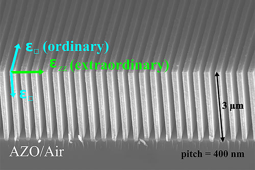 AZO trenches in air host. SEM image, bird-eye-view.
 -
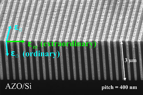 AZO trenches in Si host. SEM image, bird-eye-view.
 -
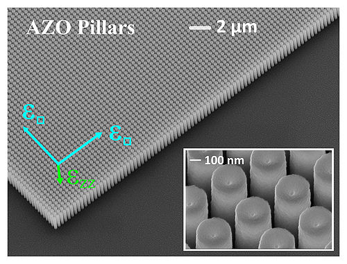 AZO pillars. SEM image, bird-eye-view.
 -
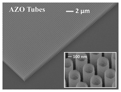 AZO tubes. SEM image, bird-eye-view.


- Optical performance of fabricated metamaterials based on Al-doped ZnO (AZO)
-
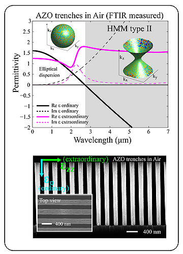 AZO trenches in air host. Enters hyperbolic regime for
 -
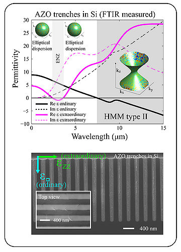 AZO trenches in Si host. Enters hyperbolic regime for
 -
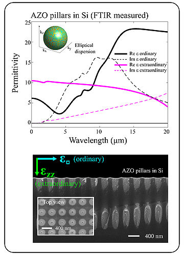 AZO pillars in Si host. Metamaterial with high anisotropy in permittivity (not HMM).
 -
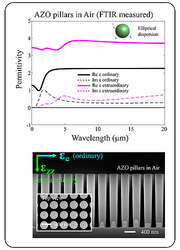 AZO pillars in Si host. Metamaterial with high anisotropy in permittivity (not HMM).


Publications in peer-review journals
Midinfrared Surface Waves on a High Aspect Ratio Nanotrench Platform
O. Takayama, E. Shkondin, A. Bogdanov, M. E. Aryaee Panah, K. Golenicki, P. Dmitriev, T. Repän, R. Malureanu, P. Belov, F. Jensen & A. Lavrinenko. ACS Photonics, 2017, 4 (11), pp 2899–2907 LINK
Large-Scale High Aspect Ratio Al-Doped ZnO Nanopillars Arrays as Anisotropic Metamaterials
E. Shkondin, O. Takayama, M. E. Aryaee Panah, P. Liu, P. V. Larsen, M. D. Mar, F. Jensen. & A. Lavrinenko (2017). Optical Materials Express, 7(5), pp. 1606-1627 (2017) LINK
Laguerre-Gauss Beam Generation in IR and UV by Subwavelength Surface-Relief Gratings
L. Vertchenko, E. Shkondin, R. Malureanu, & C. Monken (2017). Optics Express, 25(6), pp. 5917-5926 (2017) LINK
Fabrication of High Aspect Ratio TiO2 and Al2O3 Nanogratings by Atomic Layer Deposition
E. Shkondin, O. Takayama, J. Lindhard, P. V. Larsen, M. D. Mar, F. Jensen & A. Lavrinenko (2016). Journal of Vacuum Science and Technology A, 34, 031605 (2016) LINK
Experimental Demonstration of Effective Medium Approximation Breakdown in Deeply Subwavelength All-Dielectric Multilayers
S. Zhukovsky, A. Andryieuski, O. Takayama, E. Shkondin, R. Malureanu, F. Jensen, & A. Lavrinenko (2015). Physical Review Letters, 115(17), 177402 LINK
Publications in proceedings
Effective medium approximation for deeply subwavelength all-dielectric multilayers: when does it break down?
A. Lavrinenko, S. Zhukovsky, A. Andryieuski, O. Takayama, E. Shkondin, R. Malureanu and F. Jensen
Proceedings of SPIE. Vol. 9883 SPIE - International Society for Optical Engineering, (2016)
Fabrication of deep-profile Al-doped ZnO one- and two-dimensional lattices as plasmonic elements
F. Jensen, E. Shkondin, O. Takayama, P. V. Larsen, M. D. Mar, R. Malureanu, A. V. Lavrinenko
Proceedings of SPIE. Vol. 9921 SPIE - International Society for Optical Engineering, (2016)
Hyperbolic metamaterials with complex geometry
A. V. Lavrinenko, A. Andryieuski, S. Zhukovsky, O. Takayama, E. Skhondin, M. E. Aryaee Panah, R. Malureanu, F. Jensen
META'16, The 6th International Conference on Metamaterials, Photonic Crystals and Plasmonics, Malaga, Spain, 2A23, Proceedings, p.471-472 (2016)
Surface waves on metal-dielectric metamaterials
O. Takayama, E. Shkondin, M. E. Aryaee Panah, T. Repän, R. Malureanu, F. Jensen, A. V. Lavrinenko
Proceedings of 18th International Conference on Transparent Optical Networks. IEEE, (2016)
Surface waves on metamaterials interfaces
O. Takayama, E. Shkondin, M. E. Aryaee Panah, T. Repän, R. Malureanu, F. Jensen, A. V. Lavrinenko
Proceedings of 10th International Congress on Advanced Electromagnetic Materials in Microwaves and Optics.(2016)
Ultra-thin metal and dielectric layers for nanophotonic applications
E. Shkondin, L. Leandro, R. Malureanu, F. Jensen, N. Rozlosnik, A. V. Lavrinenko
Proceedings of ICTON, IEEE, 7193380. (2015)
Conferences and workshops
Conductive oxides trench structures as hyperbolic metamaterials in mid-infrared range
O. Takayama, E. Shkondin, M. E. A. Panah, T. Reän, R. Malureanu, F. Jensen, A. V. Lavrinenko
2016. Abstract from 14th International Conference of Near-Field Optics, Nanophotonics and Related Techniques, Hamamatsu, Japan
Fabrication of hollow coaxial ZnAl2O4 high aspect ratio freestanding nanopillars based on the Kirkendall effect
E. Shkondin, F. Jensen, A. V. Lavrinenko
2016. Abstract from 42nd Micro and Nano Engineering 2016, Vienna, Austria
Fabrication of Al-doped ZnO high aspect ratio nanowires and trenches as active components in mid-infrared plasmonics
E. Shkondin, O. Takayama, P. V. Larsen, M. D. Mar, F. Jensen, A. V. Lavrinenko
2016. Abstract from 16th Atomic Layer Deposition Conference, Dublin, Ireland.
TiO2 and Al2O3 ALD grown multilayers for subwavelength photonics
E. Shkondin, F. Jensen, A. V. Lavrinenko, M. D. Mar, P. V. Larsen, R. Malureanu, S. Zhukovsky, A. Andryieuski, O. Takayama
2015. DTU's Sustain Conference 2015, Technical University of Denmark, Kgs. Lyngby, Denmark (2015)
Deep subwavelength photonic multilayers fabricated by atomic layer deposition
E. Shkondin, S. Zhukovsky, A. Andryieuski, O. Takayama, R. Malureanu, M. D. Mar, A. V. Lavrinenko, F. Jensen
2015. Paper presented at 41st International conference on Micro and Nano Engineering, The Hague, Netherlands.
Fabrication of TiO2 and Al2O3 High Aspect Ratio Nanostructured Gratings at Sub-Micrometer Scale
E. Shkondin, J. M. Lindhard, M. D. Mar, F. Jensen, A. V. Lavrinenko
2015. Paper presented at 15th International Conference on Atomic Layer Deposition, Portland, Oregon, United States
Depositing Materials on the Micro- and Nanoscale
M. D. Mar, B. Herstrøm, E. Shkondin, P. Pholprasit, F. Jensen
2014. DTU's Sustain Conference 2014, Technical University of Denmark, Kgs. Lyngby, Denmark (2014)