Specific Process Knowledge/Thin film deposition/MVD: Difference between revisions
No edit summary |
|||
| (4 intermediate revisions by 3 users not shown) | |||
| Line 1: | Line 1: | ||
{{cc-nanolab}} | |||
[[Category: Equipment|Thin film MVD]] | '''Feedback to this page''': '''[mailto:photolith@nanolab.dtu.dk?Subject=Feed%20back%20from%20page%20http://labadviser.nanolab.dtu.dk/index.php/Specific_Process_Knowledge/Thin_film_deposition/MVD click here]''' | ||
[[Category: Thin Film Deposition|MVD]] | |||
[[index.php?title=Category:Equipment|Thin film MVD]] | |||
[[index.php?title=Category:Thin Film Deposition|MVD]] | |||
== The Molecular Vapor Deposition tool == | == The Molecular Vapor Deposition tool == | ||
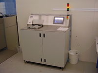
[[image:Mvd.jpg|200x200px|right|thumb|The MVD is located in cleanroom | [[image:Mvd.jpg|200x200px|right|thumb|The MVD is located in cleanroom A-1]] | ||
The Applied Microstructures MVD 100 system deposits molecular films on surfaces. These films serve a wide range of purposes ranging from antistiction coatings of nanoimprint lithography stamps to protecting MEMS structures. At DTU Nanolab the MVD is an essential tool for nanoimprint lithography, where it is used to create antistiction coatings on the imprint stamps. | |||
'''As per Jan 2025 the O2 plasma is no longer possible to use, we recommend to use a plasma asher before use and then run Flat2NP and Stamp2NP respectively, where NP is for No Plasma. - rkc''' | |||
'''The user manual, user APV, and contact information can be found in LabManager:''' | '''The user manual, user APV, and contact information can be found in LabManager:''' | ||
[http://labmanager | [http://labmanager.dtu.dk/function.php?module=Machine&view=view&mach=199 MVD in LabManager] | ||
==Process information== | ==Process information== | ||
| Line 70: | Line 75: | ||
| style="background:LightGrey; color:black"|Allowed materials | | style="background:LightGrey; color:black"|Allowed materials | ||
|style="background:WhiteSmoke; color:black" align="center" colspan="2"| | |style="background:WhiteSmoke; color:black" align="center" colspan="2"| | ||
All cleanroom materials except | All cleanroom materials except steel and other ferrous materials | ||
|- | |- | ||
|style="background:LightGrey; color:black"|Batch | |style="background:LightGrey; color:black"|Batch | ||
Latest revision as of 09:29, 8 October 2025
The content on this page, including all images and pictures, was created by DTU Nanolab staff, unless otherwise stated.
Feedback to this page: click here
The Molecular Vapor Deposition tool

The Applied Microstructures MVD 100 system deposits molecular films on surfaces. These films serve a wide range of purposes ranging from antistiction coatings of nanoimprint lithography stamps to protecting MEMS structures. At DTU Nanolab the MVD is an essential tool for nanoimprint lithography, where it is used to create antistiction coatings on the imprint stamps.
As per Jan 2025 the O2 plasma is no longer possible to use, we recommend to use a plasma asher before use and then run Flat2NP and Stamp2NP respectively, where NP is for No Plasma. - rkc
The user manual, user APV, and contact information can be found in LabManager:
Process information
| Purpose |
| ||
|---|---|---|---|
| Vapor sources | Line
|
Chemical
| |
| Performance | Contact angle |
110° (water) | |
| Process parameters | Base pressure |
20 mTorr | |
| Chamber temperature |
35°C | ||
| Chamber volume |
Approx. 3 liters | ||
| Substrates | Substrate size |
1" to 8" Smaller samples may be processed if fixed to a carrier | |
| Allowed materials |
All cleanroom materials except steel and other ferrous materials | ||
| Batch |
One sample at a time Two 4" or 6" wafers may be processed simultaneously using cassettes | ||
