Specific Process Knowledge/Characterization/Lifetime scanner MDPmap: Difference between revisions
mNo edit summary |
|||
| (18 intermediate revisions by 4 users not shown) | |||
| Line 1: | Line 1: | ||
{{cc-nanolab}} | |||
'''Feedback to this page''': '''[mailto:labadviser@danchip.dtu.dk?Subject=Feed%20back%20from%20page%20http://labadviser.danchip.dtu.dk/index.php/Specific_Process_Knowledge/Characterization/Lifetime_scanner_MDPmap click here]''' | '''Feedback to this page''': '''[mailto:labadviser@danchip.dtu.dk?Subject=Feed%20back%20from%20page%20http://labadviser.danchip.dtu.dk/index.php/Specific_Process_Knowledge/Characterization/Lifetime_scanner_MDPmap click here]''' | ||
<br> | |||
<br> | |||
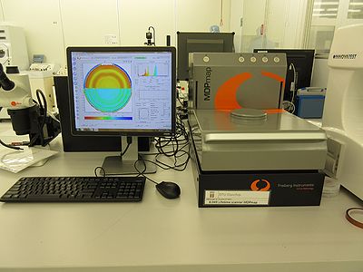
[[image:Lifetimescanner04.jpg|400x400px|right|thumb|Lifetime scanner MPDmap, positioned in cleanroom F-2.]] | |||
== Microwave Detected Photoconductivity (MDP) == | |||
Topographic visualisation of electrically active defects or materiel properties at almost any production stage, allows for process optimization and performance prediction of devices. | |||
MDP is a contact less, non destructive measurement technology for the electrical characterization | |||
of a large variety of semiconductors. The mapping and visualization of so far not detectable | |||
defects was achieved by improving the sensitivity of a microwave detection system | |||
by several orders of magnitude. Electrical properties such as lifetime, τ, mobility, μ, and diffusion | |||
length, L, can be measured also at very low injection levels with a spatial resolution limited | |||
only by the diffusion length of the charge carriers. | |||
'''The user manual, the APV and contact information can be found in LabManager:''' | |||
'''The user manual | |||
[http://labmanager.dtu.dk/function.php?module=Machine&view=view&mach=338 Lifetime scanner MPDmap info page in LabManager], | |||
== Performance information == | == Performance information == | ||
'''Range of lifetimes''': 20 ns to several ms | |||
'''The resistivity range for lifetime measurements''' 0.2 to 100 Ohm.cm, p/n | |||
'''Material''': Silicon, epitaxial layers, partially or fully processed wafers, compound semiconductors and beyond. | |||
'''Measureable properties''': Carrier lifetime (steady state or non equilibrium (µ -PCD) selectable), photoconductivity (steady state) microwave Photoconductance Decay (µ-PCD) | |||
==Equipment performance and process related parameters== | ==Equipment performance and process related parameters== | ||
| Line 21: | Line 35: | ||
!colspan="2" border="none" style="background:silver; color:black;" align="center"|Equipment | !colspan="2" border="none" style="background:silver; color:black;" align="center"|Equipment | ||
|style="background:WhiteSmoke; color:black"| | |style="background:WhiteSmoke; color:black"| <b>Lifetime scanner MDPmap </b> | ||
|- | |- | ||
!style="background:silver; color:black;" align="center" width="60"|Purpose | !style="background:silver; color:black;" align="center" width="60"|Purpose | ||
| Line 32: | Line 46: | ||
|style="background:LightGrey; color:black"| | |style="background:LightGrey; color:black"| | ||
|style="background:WhiteSmoke; color:black"| | |style="background:WhiteSmoke; color:black"| | ||
* | *Cx1 | ||
|- | |- | ||
!style="background:silver; color:black" align="center" valign="center" rowspan="2"|Instrument specifics | |||
!style="background:silver; color:black" align="center" valign="center" rowspan=" | |||
|style="background:LightGrey; color:black"|Detector | |style="background:LightGrey; color:black"|Detector | ||
|style="background:WhiteSmoke; color:black"| | |style="background:WhiteSmoke; color:black"| | ||
*Microwave detector | |||
|- | |- | ||
|style="background:LightGrey; color:black"|Laser | |style="background:LightGrey; color:black"|Laser | ||
| Line 47: | Line 58: | ||
*405 nm | *405 nm | ||
**Power 5 mW to 100 mW | **Power 5 mW to 100 mW | ||
* | *977 nm | ||
**Power 5 mW to | **Power 5 mW to 190 mW | ||
*975 nm | *975 nm | ||
**Power 0.5 W to 4.0 W | **Power 0.5 W to 4.0 W | ||
*977 nm | |||
**Power up to 200 µW | |||
*Spot diameter for all laser 0.5 µm | |||
|- | |- | ||
!style="background:silver; color:black" align="center" valign="center" rowspan="3"|Substrates | !style="background:silver; color:black" align="center" valign="center" rowspan="3"|Substrates | ||
|style="background:LightGrey; color:black"| | |style="background:LightGrey; color:black"|Size | ||
|style="background:WhiteSmoke; color:black"| | |style="background:WhiteSmoke; color:black"| | ||
* | *Sample sizs between 5 mm x 5 mm up to 16" or 210 mm x 210 mm | ||
*Sample thickness 10 µm to 20 mm | |||
* | |||
|- | |- | ||
| style="background:LightGrey; color:black"|Allowed materials | | style="background:LightGrey; color:black"|Allowed materials | ||
Latest revision as of 19:40, 27 May 2025
The content on this page, including all images and pictures, was created by DTU Nanolab staff, unless otherwise stated.
Feedback to this page: click here

Microwave Detected Photoconductivity (MDP)
Topographic visualisation of electrically active defects or materiel properties at almost any production stage, allows for process optimization and performance prediction of devices.
MDP is a contact less, non destructive measurement technology for the electrical characterization of a large variety of semiconductors. The mapping and visualization of so far not detectable defects was achieved by improving the sensitivity of a microwave detection system by several orders of magnitude. Electrical properties such as lifetime, τ, mobility, μ, and diffusion length, L, can be measured also at very low injection levels with a spatial resolution limited only by the diffusion length of the charge carriers.
The user manual, the APV and contact information can be found in LabManager:
Lifetime scanner MPDmap info page in LabManager,
Performance information
Range of lifetimes: 20 ns to several ms
The resistivity range for lifetime measurements 0.2 to 100 Ohm.cm, p/n
Material: Silicon, epitaxial layers, partially or fully processed wafers, compound semiconductors and beyond.
Measureable properties: Carrier lifetime (steady state or non equilibrium (µ -PCD) selectable), photoconductivity (steady state) microwave Photoconductance Decay (µ-PCD)
| Equipment | Lifetime scanner MDPmap | |
|---|---|---|
| Purpose |
| |
| Location |
| |
| Instrument specifics | Detector |
|
| Laser |
| |
| Substrates | Size |
|
| Allowed materials |
| |
