Specific Process Knowledge/Thin Film deposition/ALD/TiO2 deposition using ALD: Difference between revisions
mNo edit summary |
|||
| (8 intermediate revisions by 2 users not shown) | |||
| Line 1: | Line 1: | ||
{{cc-nanolab}} | |||
'''Feedback to this page''': '''[mailto:labadviser@nanolab.dtu.dk?Subject=Feed%20back%20from%20page%20http://labadviser.nanolab.dtu.dk/index.php/Specific_Process_Knowledge/Thin_Film_deposition/ALD/TiO2_deposition_using_ALD click here]''' | |||
<br> | |||
<br> | |||
The ALD window for titanium dioxide (TiO<sub>2</sub>) ranges from 120 <sup>o</sup>C to 350 <sup>o</sup>C. | The ALD window for titanium dioxide (TiO<sub>2</sub>) ranges from 120 <sup>o</sup>C to 350 <sup>o</sup>C. | ||
| Line 6: | Line 9: | ||
For Si wafers, amorphous TiO<sub>2</sub> is best grown on wafers with native oxide, and anatase TiO<sub>2</sub> is best grown on wafers without native oxide (removed using HF). | For Si wafers, amorphous TiO<sub>2</sub> is best grown on wafers with native oxide, and anatase TiO<sub>2</sub> is best grown on wafers without native oxide (removed using HF). | ||
====TiO<sub>2</sub> standard recipe==== | ====TiO<sub>2</sub> standard recipe==== | ||
| Line 32: | Line 37: | ||
|- | |- | ||
|} | |} | ||
====TiO<sub>2</sub> deposition rates==== | ====TiO<sub>2</sub> deposition rates==== | ||
| Line 42: | Line 48: | ||
image:ALD_TiO2_grow_rate_350C.jpg| Temperature 350 <sup>o</sup>C. | image:ALD_TiO2_grow_rate_350C.jpg| Temperature 350 <sup>o</sup>C. | ||
</gallery> | </gallery> | ||
Evgeniy Shkondin, DTU Nanolab (former DTU Danchip), April-May 2014. | |||
====TiO<sub>2</sub> results==== | ====TiO<sub>2</sub> results==== | ||
| Line 64: | Line 73: | ||
<br clear="all" /> | <br clear="all" /> | ||
Evgeniy Shkondin, DTU Nanolab (former DTU Danchip), 2014. | |||
====TiO<sub>2</sub> deposition on trenches==== | |||
For TiO<sub>2</sub> deposition on trenches more information can be found here: | |||
*[[Specific Process Knowledge/Thin Film deposition/ALD/TiO2 deposition using ALD/TiO2 deposition on trenches using ALD|TiO<sub>2</sub> deposition on trenches using ALD]] | |||
Latest revision as of 17:00, 21 May 2025
The content on this page, including all images and pictures, was created by DTU Nanolab staff, unless otherwise stated.
Feedback to this page: click here
The ALD window for titanium dioxide (TiO2) ranges from 120 oC to 350 oC.
A low temperatures between 120 oC and 150 oC an amorphous TiO2 layer is grown in the ALD, and at higher temperatures between 300 oC and 350 oC an anatase TiO2 layer is grown. At temperatures between 150 oC and 300 oC the TiO2 layer will be a mixture of both amorphous and anatase TiO2.
For Si wafers, amorphous TiO2 is best grown on wafers with native oxide, and anatase TiO2 is best grown on wafers without native oxide (removed using HF).
TiO2 standard recipe
Recipe: TiO2
Temperature: 120 oC - 350 oC
| TiCl4 | H2O | |
|---|---|---|
| Nitrogen flow | 150 sccm | 200 sccm |
| Pulse time | 0.1 s | 0.1 s |
| Purge time | 4.0 s | 5.0 s |
TiO2 deposition rates
In the graphs below the TiO2 thickness as function of the number of cycles for deposition temperatures between 150 oC and 350 oC can be seen. From the equations the number of cycles required for a certain thickess to be deposited can be calculated. All results have been obtained for Si wafers with native oxide.
- Titanium dioxide thickness as function of number of cycles
-
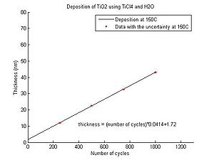 Temperature 150 oC.
 -
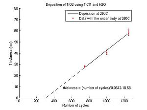 Temperature 250 oC.
 -
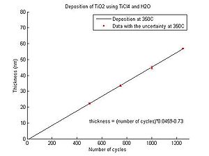 Temperature 350 oC.


Evgeniy Shkondin, DTU Nanolab (former DTU Danchip), April-May 2014.
TiO2 results
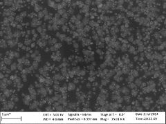
Some some SEM images of TiO2 deposited on a Si surface at different temperatures between 150 oC and 350 oC are shown below. Some of samples have been treated with HF (hydrofluoric acid) to remove the native oxide layer just before the ALD deposition.
- Titanium dioxide deposited at different temperatures on a Si surface
-
 Temperature 150 oC, 1200 cycles, HF treated.
 -
 Temperature 150 oC, 1200 cycles.
 -
 Temperature 250 oC, 750 cycles.


-
 Temperature 300 oC, 1000 cycles, HF treated.
 -
 Temperature 300 oC, 1000 cycles.
 -
 Temperature 350 oC, 1250 cycles, HF treated.


XPS measurements of TiO2 deposited at 120 oC and 300 oC are shown below. From the XPS measurements it can be calculated that at temperatures below 120 oC the TiO2 layer will be contaminated with about 1-3 % chlorine molecules from the TiCl4 precursor. This can be also seen as small white dots in the SEM image of the amorphous TiO2 layers above.

Evgeniy Shkondin, DTU Nanolab (former DTU Danchip), 2014.
TiO2 deposition on trenches
For TiO2 deposition on trenches more information can be found here: