Specific Process Knowledge/Characterization/Sample preparation: Difference between revisions
mNo edit summary |
|||
| (44 intermediate revisions by 3 users not shown) | |||
| Line 1: | Line 1: | ||
=Replica Molding for Sample Inspection= | |||
''by Frederik Stöhr, DTU Nanolab (former DTU Danchip), May 2015'' | |||
==Introduction== | |||
* A simplified list of necessary steps is given below | Negative replicas of micro- or nanostructures can be obtained by casting with PDMS. This can facilitate the characterization of the three dimensional shape, the texture, or the roughness of a given sample. It may circumvent the inabilities of probes (AFM tip, stylus) to approach a surface of e.g. a deep and narrow cavity. It may also circumvent limitations of the optical profiler regarding the maximum detectable slope or the sensitivity of the CCD when measuring strongly tapered or deep cavities. PDMS is a common material in microfabrication and has unique properties that allow replicating features in the single nanometer range [[http://pubs.acs.org/doi/abs/10.1021/nl048355u 1]]. | ||
* A simplified list of necessary steps is given below | |||
* Please follow the safety and working rules of the individual lab the work is done in and consider the safety instructions given in [[http://www.nature.com/nprot/journal/v5/n3/full/nprot.2009.234.html 2]]. | |||
* There is a dedicated lab for work with PDMS at DTU Nanotech (not sure where it is now 2019-06-26). | |||
* Please be aware that it is not allowed to work with PDMS in its uncured state inside the cleanroom. The list of approved chemicals inside the cleanroom still holds. | * Please be aware that it is not allowed to work with PDMS in its uncured state inside the cleanroom. The list of approved chemicals inside the cleanroom still holds. | ||
* Details on | * Details on our experience with PDMS as a casting material may be found in [[http://www.sciencedirect.com/science/article/pii/S0167931714005322 3]] (please cite!). A detailed description for PDMS casting can be found in [[http://www.nature.com/nprot/journal/v5/n3/full/nprot.2009.234.html 2]] and practical information is given in [[http://www.elveflow.com/microfluidic-tutorials/soft-lithography-reviews-and-tutorials/introduction-in-soft-lithography/pdms-softlithography-replication/ 4]]. | ||
* The most important steps for obtaining high quality casts are the thorough mixing of the two components of the PDMS Kit (Sylgard 184, Dow Corning) and the sufficient outgassing of the polymer prior and after pouring the polymer into the mould. The house vacuum may be too weak. For special demands, try to get hold of a separate pump like a HiCube Classic from Pfeiffer Vacuum [ | * The most important steps for obtaining high quality casts are the thorough mixing of the two components of the PDMS Kit (Sylgard 184, Dow Corning) and the sufficient outgassing of the polymer prior and after pouring the polymer into the mould. The house vacuum may be too weak. For special demands, try to get hold of a separate pump like a HiCube Classic from Pfeiffer Vacuum [[http://www.sciencedirect.com/science/article/pii/S0167931708004656 5]] (there is one around at DTU Photonics or DTU Nanolab (former DTU Danchip)). | ||
* The application of an anti-stiction coating, like FDTS, is necessary. It may be applied inside the cleanroom by the MVD. Contact the respective person. | * The application of an anti-stiction coating, like FDTS, is necessary. It may be applied inside the cleanroom by the MVD. Contact the respective person. | ||
* The mold may be reused upon casting without deterioration (try!) | * The mold may be reused upon casting without deterioration (try!) | ||
| Line 64: | Line 69: | ||
|style="background:WhiteSmoke; color:black"|Gently detach the cured PDMS from the mold. | |style="background:WhiteSmoke; color:black"|Gently detach the cured PDMS from the mold. | ||
|- | |- | ||
|} | |||
<br clear="all" /> | |||
==Example: Replica Molding of cross sections of DRIE etched cavities== | |||
'''General Description'''<br> | |||
As exemplified in [[http://www.sciencedirect.com/science/article/pii/S0167931714005322 3]] the three-dimensional shape of deep reactive ion etched cavities in silicon have been characterized by replica molding and atomic force microscopy (please cite!). Neither AFM directly, nor the optical profiler was able to do the job due to reasons explained above. The procedure proofed to be extremely reliable and accurate. | |||
{| border="1" cellspacing="1" cellpadding="1" align="middle" | |||
![[image:SEM_SliceCrossection_1.jpg|300x300px|thumb|left| | |||
Cross section of a silicon wafer with a multitude of deep reactive ion etched cavities. The shape of these cavities is of interest. | |||
]] | |||
![[image:SEM_SliceCrossection_2.jpg|300x300px|thumb|left| | |||
Close up. The feature has a cylindric-parabolic shape and steep sidewalls. The target is to measure the parabolic shape along the depth of the features. | |||
]] | |||
|- | |||
|} | |||
{| border="1" cellspacing="1" cellpadding="1" align="middle" | |||
![[image:StackedSlices_2.jpg|300x300px|thumb|left| | |||
Photograph of a multitude of silicon slices stacked and fixed with a purpose made clamp made of Aluminum. Attention must be payed to the straightness of the slices and the proper stacking of them, so they can be casted nicely. | |||
]] | |||
![[image:StackedSlices_3.jpg|300x300px|thumb|left| | |||
Close up. The DRIE etched cavities are visible. The edges of the slices are almost in one plane, allowing nice casting. | |||
]] | |||
![[image:StackedSlicesWithFrame.jpg|300x300px|thumb|left| | |||
In order to be able to fill the cavities with PDMS and obtain a proper sample a fixture needs to be placed on top of the features. The gap between clamp and fixture needs to be carefully sealed with e.g. sticky tape. | |||
]] | |||
|- | |||
|} | |||
{| border="1" cellspacing="1" cellpadding="1" align="middle" | |||
![[image:WaferWithCast_2.jpg|300x300px|thumb|left| | |||
Photograph of the temperature cured and released PDMS sample fixed to a silicon wafer ready for further inspection. | |||
]] | |||
![[image:Cast.jpg|300x300px|thumb|left| | |||
Close up showing the replicated features in PDMS. | |||
]] | |||
|- | |||
|} | |||
{| border="1" cellspacing="1" cellpadding="1" align="middle" | |||
![[image:SEM_PDMS_1.jpg|300x300px|thumb|left| | |||
SEM showing the replicated features in PDMS. | |||
]] | |||
![[image:SEM_PDMS_2.jpg|300x300px|thumb|left| | |||
SEM showing the replicated features in PDMS. | |||
]] | |||
![[image:SEM_PDMS_3.jpg|300x300px|thumb|left| | |||
Close up. SEM showing a replicated feature in PDMS. | |||
]] | |||
|- | |||
|} | |||
{| border="1" cellspacing="1" cellpadding="1" align="middle" | |||
![[image:SEM_PDMS_4.jpg|300x300px|thumb|left| | |||
SEM showing a replicated feature in PDMS. | |||
]] | |||
![[image:SEM_PDMS_5.jpg|300x300px|thumb|left| | |||
SEM showing a replicated feature in PDMS. | |||
]] | |||
|- | |||
|} | |||
{| border="1" cellspacing="1" cellpadding="1" align="middle" | |||
![[image:AFM-PDMS_BOTH_4.jpg|300x300px|thumb|left| | |||
Concept of AFM profiling. (a) 3D view of one of the feature and axis assignment. (b) Front view of one of the casted feature with approached AFM tip. The AFM tip and the PDMS feature are to the same scale. The geometry of an inverted KOH etched silicon V-groove is superposed and indicated by the dotted red lines. | |||
]] | |||
|- | |||
|} | |} | ||
<br clear="all" /> | |||
<br clear="all" /> | <br clear="all" /> | ||
==References== | ==References== | ||
[http://www. | [1] [http://pubs.acs.org/doi/abs/10.1021/nl048355u Polymer Imprint Lithography with Molecular-Scale Resolution] | ||
[2] [http://www.nature.com/nprot/journal/v5/n3/full/nprot.2009.234.html Soft lithography for micro- and nanoscale patterning] | |||
[3] [http://www.sciencedirect.com/science/article/pii/S0167931714005322 Three-dimensional nanometrology of microstructures by replica molding and large-range atomic force microscopy] | |||
[4] [http://www.elveflow.com/microfluidic-tutorials/soft-lithography-reviews-and-tutorials/introduction-in-soft-lithography/pdms-softlithography-replication/ How to do PDMS lithography replication from a SU-8 mold?] | |||
[5] [http://www.sciencedirect.com/science/article/pii/S0167931708004656 Research on the cast molding process for high quality PDMS molds] | |||
Latest revision as of 16:53, 21 May 2025
Replica Molding for Sample Inspection
by Frederik Stöhr, DTU Nanolab (former DTU Danchip), May 2015
Introduction
Negative replicas of micro- or nanostructures can be obtained by casting with PDMS. This can facilitate the characterization of the three dimensional shape, the texture, or the roughness of a given sample. It may circumvent the inabilities of probes (AFM tip, stylus) to approach a surface of e.g. a deep and narrow cavity. It may also circumvent limitations of the optical profiler regarding the maximum detectable slope or the sensitivity of the CCD when measuring strongly tapered or deep cavities. PDMS is a common material in microfabrication and has unique properties that allow replicating features in the single nanometer range [1].
- A simplified list of necessary steps is given below
- Please follow the safety and working rules of the individual lab the work is done in and consider the safety instructions given in [2].
- There is a dedicated lab for work with PDMS at DTU Nanotech (not sure where it is now 2019-06-26).
- Please be aware that it is not allowed to work with PDMS in its uncured state inside the cleanroom. The list of approved chemicals inside the cleanroom still holds.
- Details on our experience with PDMS as a casting material may be found in [3] (please cite!). A detailed description for PDMS casting can be found in [2] and practical information is given in [4].
- The most important steps for obtaining high quality casts are the thorough mixing of the two components of the PDMS Kit (Sylgard 184, Dow Corning) and the sufficient outgassing of the polymer prior and after pouring the polymer into the mould. The house vacuum may be too weak. For special demands, try to get hold of a separate pump like a HiCube Classic from Pfeiffer Vacuum [5] (there is one around at DTU Photonics or DTU Nanolab (former DTU Danchip)).
- The application of an anti-stiction coating, like FDTS, is necessary. It may be applied inside the cleanroom by the MVD. Contact the respective person.
- The mold may be reused upon casting without deterioration (try!)
A simplified list of necessary steps
| Step | Task | Aim | Methods |
|---|---|---|---|
| 1 | Sample preparation | A mold containing the sample that is sufficiently sealed to allow holding the viscous polymer. | Some parts from the mechanical workshop, etc. Do not forget poper cleaning. |
| 2 | Anti-stiction coating | A sample to which PDMS does not adhere upon casting. | E.g. MVD -> FDTS layer (comply to cleanroom and machine rules) |
| 3 | PDMS mixing | A good PDMS mixture. | The kit, a plastic cup, a spatula and patience. |
| 4 | Mixture Outgassing | A mixture without any air bubbles apparent. | A desiccator. (~10min) |
| 5 | Pouring | The mixture is filled into the structures to be casted. | Gently pour the mixture into the mold. |
| 6 | Sample outgassing. | A sample filled with the mixture without air being trapped somewhere. | A desiccator. (~10min) |
| 7 | Sample curing | A cured PDMS. | An oven (e.g. 5 hours @ 70C) |
| 8 | Sample cooling | A cooled PDMS & sample | ~3 hours @ room temperature |
| 9 | PDMS release | The PDMS cast ready for further usage | Gently detach the cured PDMS from the mold. |
Example: Replica Molding of cross sections of DRIE etched cavities
General Description
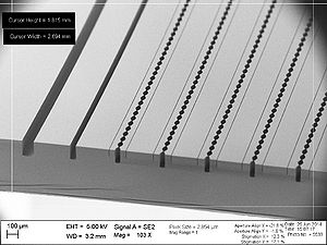
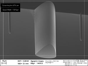
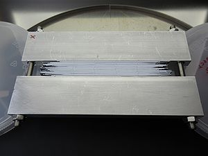
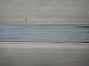
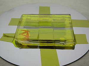
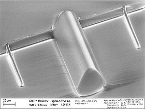
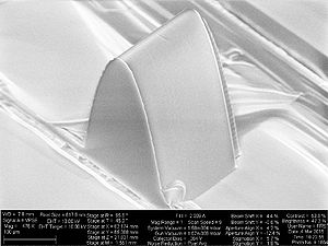
As exemplified in [3] the three-dimensional shape of deep reactive ion etched cavities in silicon have been characterized by replica molding and atomic force microscopy (please cite!). Neither AFM directly, nor the optical profiler was able to do the job due to reasons explained above. The procedure proofed to be extremely reliable and accurate.
 |
 |
|---|
 |
 |
 |
|---|
 |
 |
|---|
References
[1] Polymer Imprint Lithography with Molecular-Scale Resolution
[2] Soft lithography for micro- and nanoscale patterning
[4] How to do PDMS lithography replication from a SU-8 mold?
[5] Research on the cast molding process for high quality PDMS molds

