Specific Process Knowledge/Etch/DRIE-Pegasus/nanoetch/nano142: Difference between revisions
No edit summary |
No edit summary |
||
| (13 intermediate revisions by 2 users not shown) | |||
| Line 1: | Line 1: | ||
'''Feedback to this page''': '''[mailto:labadviser@ | '''Feedback to this page''': '''[mailto:labadviser@nanolab.dtu.dk?Subject=Feed%20back%20from%20page%20http://labadviser.nanolab.dtu.dk/index.php/Specific_Process_Knowledge/Etch/DRIE-Pegasus/nanoetch/nano142 click here]''' | ||
<!--Checked for updates on 30/7-2018 - ok/jmli --> | |||
<!--Checked for updates on 5/10-2020 - ok/jmli --> | |||
<!--Checked for updates on 4/9-2025 - ok/jmli --> | |||
== The nano1.42 recipe == | == The nano1.42 recipe == | ||
{{Template:Author-jmli1}} | |||
<!--Checked for updates on 2/02-2023 - ok/jmli --> | |||
{| border="2" cellpadding="2" cellspacing="1" | {| border="2" cellpadding="2" cellspacing="1" | ||
| Line 77: | Line 81: | ||
| | | | ||
|} | |} | ||
==Etching SRN (Silicon Rich Nitride) with nano1.42== | |||
''This test has been done by Leonid Beliaev'' <br> | |||
*274nm SRN by LPCVD ("6 inch LS" recipe) | |||
*Substrate: Si/SiO2(1100nm) | |||
*DUV-lithography: KRF M230Y resist 360 nm, Barc 65 nm, exposure dose 220J/m2 | |||
*Pattern: Grating with period 400 nm and grating bar width of | |||
*Barc etch in Pegasus 1 at -19 deg, 40s | |||
*Nano 1.42 at -19 deg, 5 min | |||
[[File:Etch_rate.png|400px]] | |||
[[File:Test_007.jpg|400px|left|thumb|Image: Leonid Beliaev]] | |||
Latest revision as of 12:01, 4 September 2025
Feedback to this page: click here
The nano1.42 recipe
Unless otherwise stated, all content on this page was created by Jonas Michael-Lindhard, DTU Nanolab
| Recipe | Gas | C4F8 75 sccm, SF6 38 sccm |
|---|---|---|
| Pressure | 4 mTorr, Strike 3 secs @ 15 mTorr | |
| Power | 800 W CP, 40 W PP | |
| Temperature | -20 degs | |
| Hardware | 100 mm Spacers | |
| Time | 120 secs | |
| Conditions | Run ID | 2017 |
| Conditioning | Sequence: Oxygen clean, MU tests, processes, no oxygen between runs | |
| Mask | 211 nm zep etched down to 82 nm |
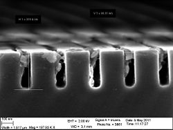
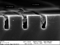
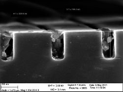
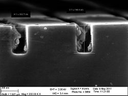
- The results of the nano1.42 recipe
-
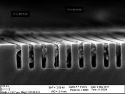 The 30 nm trenches
 -
 The 60 nm trenches
 -
 The 90 nm trenches
 -
 The 120 nm trenches
 -
 The 150 nm trenches


| Nominal trench line width | ' | 30 | 60 | 90 | 120 | 150 | Average | Std. dev. |
| Etch rates | nm/min | 148 | 158 | 164 | 167 | 166 | 160 | 8 |
| Sidewall angle | degs | 90 | 90 | 90 | 90 | 90 | 90 | 0 |
| CD loss | nm/edge | 7 | -7 | -7 | -28 | -28 | -13 | 15 |
| CD loss foot | nm/edge | 12 | 5 | 6 | -15 | -1 | 1 | 10 |
| Bowing | -1 | 1 | -2 | -5 | -7 | -3 | 3 | |
| Bottom curvature | -46 | -30 | -29 | -31 | -27 | -32 | 8 | |
| zep | nm/min | 65 | ||||||
Etching SRN (Silicon Rich Nitride) with nano1.42
This test has been done by Leonid Beliaev
- 274nm SRN by LPCVD ("6 inch LS" recipe)
- Substrate: Si/SiO2(1100nm)
- DUV-lithography: KRF M230Y resist 360 nm, Barc 65 nm, exposure dose 220J/m2
- Pattern: Grating with period 400 nm and grating bar width of
- Barc etch in Pegasus 1 at -19 deg, 40s
- Nano 1.42 at -19 deg, 5 min

