|
|
| (11 intermediate revisions by 2 users not shown) |
| Line 7: |
Line 7: |
| {{Template:Author-jmli1}} | | {{Template:Author-jmli1}} |
| <!--Checked for updates on 2/02-2023 - ok/jmli --> | | <!--Checked for updates on 2/02-2023 - ok/jmli --> |
| | <!--Checked for updates on 21/10-2025 - ok/jmli --> |
|
| |
|
| In 2010 DTU Nanolab acquired DRIE-Pegasus 1 (at the time called Danchip and DRIE-Pegasus, respectively). As a state-of-the-art etch tool with excellent performance and great flexibility, it grew immensely popular and by 2015 it was apparent that we needed yet another tool to cope with the demand. Therefore, in 2016 Pegasus 2 was acquired from a closed-down lab in Morocco and installed next to Pegasus 1. | | In 2010 DTU Nanolab acquired DRIE-Pegasus 1. As a state-of-the-art etch tool with excellent performance and great flexibility, it grew immensely popular and by 2015 it was apparent that we needed yet another tool to cope with the demand. Therefore, in 2016 Pegasus 2 was acquired from a closed-down lab and installed next to Pegasus 1. |
|
| |
|
| Looking to expand our dry etching capabilities in 2017 we got an irresistible offer on a twin Pegasus system with cassette to cassette vacuum robot from a commerciel fab. The twin Pegasus system (called Pegasus 3 and 4) is installed at the old cluster 2 location in cleanroom C1 and will run only 6" wafers. Pegasus 3 is the 6" silicon etch work horse and Pegasus 4 is converted (adding extra process gases) into a 6" dielectric etch tool that will supplement/replace the AOE. | | Looking to expand our dry etching capabilities in 2017 we got an irresistible offer on a twin Pegasus system with cassette to cassette vacuum robot from a commercial fab. The twin Pegasus system (called Pegasus 3 and 4) is installed at the old cluster 2 location in cleanroom C1 and will run only 6" wafers. Pegasus 3 is the 6" silicon etch work horse and Pegasus 4 is converted (adding extra process gases) into a 6" dielectric etch tool that will supplement/replace the AOE. |
|
| |
|
| This page was originally intended as a regular one-machine page (the Pegasus 1 page). However, as of 2018 with several tools, the page will serve as common page for all of our Pegasi with subpages for each tool. | | This page was originally intended as a regular one-machine page (the Pegasus 1 page). However, as of 2018 with several tools, the page will serve as common page for all of our Pegasi with subpages for each tool. |
|
| |
|
| {| | | {| |
| |width="200"| [[file:DRIE-Pegasus.jpg |200px|frameless]] | | |width="100"| [[file:DRIE-Pegasus.jpg |100px|frameless]] |
| | width="400"| [[file:Pegasus 2 operator.jpg |408px|frameless]] | | | width="200"| [[file:Pegasus 2 operator.jpg |204px|frameless]] |
| | width="550"|[[file:Peg3and4 front 2.JPG |584px|frameless]] | | | width="275"|[[file:Peg3and4 front 2.JPG |292px|frameless]] |
| |- | | |- |
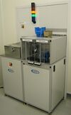
| | align="center" | The DRIE-Pegasus 1 load lock and cassette loader in the DTU Nanolab cleanroom A-1. {{photo1}} | | | align="center" | The DRIE-Pegasus 1 load lock and cassette loader in the DTU Nanolab cleanroom A-1. {{photo1}} |
| Line 120: |
Line 121: |
| * Ar: 0 to 283 sccm | | * Ar: 0 to 283 sccm |
| |style="background:lightgrey; color:black"| | | |style="background:lightgrey; color:black"| |
| * SF<sub>6</sub>: 0 to 1200 sccm | | * SF<sub>6</sub>-1: 0 to 1200 sccm |
| | * SF<sub>6</sub>-2: 0 to 100 sccm |
| | * O<sub>2</sub>: 0 to 50 sccm |
| | * N<sub>2</sub>: 0 to 500 sccm |
| | * Ar: 0 to 283 sccm |
| | * He: 0 to 11 sccm |
| | |style="background:lightgrey; color:black"| |
| | * SF<sub>6</sub>-1: 0 to 1200 sccm |
| | * SF<sub>6</sub>-2: 0 to 100 sccm |
| * O<sub>2</sub>: 0 to 200 sccm | | * O<sub>2</sub>: 0 to 200 sccm |
| * C<sub>4</sub>F<sub>8</sub>: 0 to 400 sccm | | * C<sub>4</sub>F<sub>8</sub>: 0 to 400 sccm |
| * Ar: 0 to 283 sccm | | * Ar: 0 to 283 sccm |
| |style="background:lightgrey; color:black"|
| |
| * SF<sub>6</sub>
| |
| * O<sub>2</sub>
| |
| * C<sub>4</sub>F<sub>8</sub>
| |
| * Ar
| |
| |style="background:lightgrey; color:black"| | | |style="background:lightgrey; color:black"| |
| {| | | {| |
| Line 254: |
Line 258: |
|
| |
|
|
| |
|
|
| |
| ==Comparison of SEM's in building 346/451==
| |
|
| |
| {| border="2" cellspacing="0" cellpadding="0"
| |
| !colspan="2" border="none" style="background:silver; color:black;" align="center"|Equipment
| |
| |style="background:WhiteSmoke; color:black" align="center"|[[Specific_Process_Knowledge/Characterization/SEM_Supra_1|SEM Supra 1]]
| |
| |style="background:WhiteSmoke; color:black" align="center"|[[Specific_Process_Knowledge/Characterization/SEM_Supra_2|SEM Supra 2]]
| |
| |style="background:WhiteSmoke; color:black" align="center"|[[Specific_Process_Knowledge/Characterization/SEM_Supra_3|SEM Supra 3]]
| |
| <i>Under installation (August 2023)</i>
| |
| |style="background:WhiteSmoke; color:black" align="center"|[[Specific_Process_Knowledge/Characterization/SEM_Tabletop_1|SEM Tabletop 1]]
| |
| <!--|style="background:WhiteSmoke; color:black" align="center"|[[Specific Process Knowledge/Characterization/SEM FEI QUANTA 200 3D|FEI Quanta 200 3D]]-->
| |
| |-
| |
| !colspan="2" border="none" style="background:silver; color:black;" align="center"|Model
| |
| |style="background:WhiteSmoke; color:black" align="center"| Zeiss Supra 40 VP
| |
| |style="background:WhiteSmoke; color:black" align="center"| Zeiss Supra 60 VP
| |
| |style="background:WhiteSmoke; color:black" align="center"| Zeiss Supra 40 VP
| |
| |style="background:WhiteSmoke; color:black" align="center"| SEM Tabletop 1
| |
| <!--|style="background:WhiteSmoke; color:black" align="center"| FEI Quanta 200 3D-->
| |
| |-
| |
| !style="background:silver; color:black" align="center" valign="center" rowspan="2"|Purpose
| |
| |style="background:LightGrey; color:black" align="center" | Imaging and measurement of
| |
| |style="background:WhiteSmoke; color:black"|
| |
| * Conducting samples
| |
| * Semi-conducting samples
| |
| * Thin (~ 5 µm <) layers of non-conducting materials such as polymers
| |
| * Thick polymers, glass or quartz samples
| |
| |style="background:WhiteSmoke; color:black"|
| |
| * Conducting samples
| |
| * Semi-conducting samples
| |
| * Thin (~ 5 µm <) layers of non-conducting materials such as polymers
| |
| * Thick polymers, glass or quartz samples
| |
| |style="background:WhiteSmoke; color:black"|
| |
| * Conducting samples
| |
| * Semi-conducting samples
| |
| * Thin (~ 5 µm <) layers of non-conducting materials such as polymers
| |
| * Thick polymers, glass or quartz samples
| |
| |style="background:WhiteSmoke; color:black"|
| |
| * Conducting samples
| |
| * Semi-conducting samples
| |
| * Thin (~ 5 µm <) layers of non-conducting materials such as polymers
| |
| * Thick polymers, glass or quartz samples
| |
| <!--|style="background:WhiteSmoke; color:black"|
| |
| * Conductive samples-->
| |
| |-
| |
| |style="background:LightGrey; color:black" align="center" |Other purpose
| |
| |style="background:WhiteSmoke; color:black"| <!-- comment -->
| |
| |style="background:WhiteSmoke; color:black"|
| |
| * Surface material analysis using EDX
| |
| |style="background:WhiteSmoke; color:black"|
| |
| |style="background:WhiteSmoke; color:black"|
| |
| |style="background:WhiteSmoke; color:black"|
| |
| |-
| |
| !style="background:silver; color:black;" align="center" width="60"|Instrument location
| |
| |style="background:LightGrey; color:black"|
| |
| |style="background:WhiteSmoke; color:black"|
| |
| *Basement of building 346
| |
| |style="background:WhiteSmoke; color:black"|
| |
| *Cleanroom of DTU Nanolab in building 346
| |
| |style="background:WhiteSmoke; color:black"|
| |
| *Cleanroom of DTU Nanolab in building 346
| |
| |style="background:WhiteSmoke; color:black"|
| |
| *Building 451 - room 913
| |
| (in the North-East corner of the building's basement)
| |
| <!--|style="background:WhiteSmoke; color:black"|
| |
| *DTU CEN-->
| |
|
| |
| |-
| |
| !style="background:silver; color:black" align="center" valign="center" rowspan="2"|Performance
| |
| |style="background:LightGrey; color:black" rowspan="2" align="center" |Resolution
| |
| |style="background:Whitesmoke; color:black" colspan="5" align="center"| The resolution of a SEM is strongly dependent on the type of sample and the skills of the operator. The highest resolution is probably only achieved on special samples
| |
| |-
| |
| |style="background:WhiteSmoke; color:black"|
| |
| * 1-2 nm (limited by vibrations)
| |
| |style="background:WhiteSmoke; color:black"|
| |
| * 1-2 nm (limited by vibrations)
| |
| |style="background:WhiteSmoke; color:black"|
| |
| * 1-2 nm (limited by vibrations)
| |
|
| |
| <!--|style="background:WhiteSmoke; color:black"|
| |
| * ~3.5 nm (limited by instrument)-->
| |
| |style="background:WhiteSmoke; color:black"|
| |
| * ~25 nm (limited by instrument)
| |
| |-
| |
| !style="background:silver; color:black" align="center" valign="center" rowspan="5"|Instrument specifics
| |
| |style="background:LightGrey; color:black" align="center" |Detectors
| |
| |style="background:WhiteSmoke; color:black"|
| |
| * Secondary electron (Se2)
| |
| * Inlens secondary electron (Inlens)
| |
| * 4 Quadrant Backscatter electron (QBSD)
| |
| * Variable pressure secondary electron (VPSE)
| |
| |style="background:WhiteSmoke; color:black"|
| |
| * Secondary electron (Se2)
| |
| * Inlens secondary electron (Inlens)
| |
| * 4 Quadrant Backscatter electron (QBSD)
| |
| * Variable pressure secondary electron (VPSE)
| |
| |style="background:WhiteSmoke; color:black"|
| |
| * Secondary electron (Se2)
| |
| * Inlens secondary electron (Inlens)
| |
| * High Definition four quadrant Angular Selective Backscattered electron detector (HDAsB)
| |
| * Variable pressure secondary electron (VPSE)
| |
|
| |
| <!--|style="background:WhiteSmoke; color:black"|
| |
| * Secondary electron (Everhart-Thornley (ETD))
| |
| * Backscatter electron (BSD) - Add-on
| |
| * Large Field Detector (LFD) - Add-on
| |
| * CCD camera -->
| |
| |style="background:WhiteSmoke; color:black"|
| |
| * Secondary electron (SE)
| |
| * Backscatter electron (BSE)
| |
| |-
| |
| |style="background:LightGrey; color:black" align="center" |Stage
| |
| |style="background:WhiteSmoke; color:black"|
| |
| * X, Y: 130 × 130 mm
| |
| * T: -4 to 70<sup>o</sup>
| |
| * R: 360<sup>o</sup>
| |
| * Z: 50 mm
| |
| |style="background:WhiteSmoke; color:black"|
| |
| * X, Y: 150 × 150 mm
| |
| * T: -10 to 70<sup>o</sup>
| |
| * R: 360<sup>o</sup>
| |
| * Z: 50 mm
| |
| |style="background:WhiteSmoke; color:black"|
| |
| * X, Y: 130 × 130 mm
| |
| * T: -4 to 70<sup>o</sup>
| |
| * R: 360<sup>o</sup>
| |
| * Z: 50 mm
| |
| |style="background:WhiteSmoke; color:black"|
| |
| * X, Y: 35 mm
| |
| * T: No tilt
| |
| * R: No rotation
| |
| * Z: 0 mm
| |
| |-
| |
| |style="background:LightGrey; color:black" align="center" |Electron source
| |
| |style="background:Whitesmoke; color:black" colspan="4" align="center"| FEG (Field Emission Gun) source
| |
| |style="background:WhiteSmoke; color:black"|
| |
| * Thermionic tungsten filament
| |
| <!--|style="background:WhiteSmoke; color:black"|
| |
| * Tungsten filament-->
| |
| |-
| |
| |style="background:LightGrey; color:black" align="center" |Operating pressures
| |
| |style="background:WhiteSmoke; color:black"|
| |
| * Fixed at High vacuum (2 × 10<sup>-4</sup>mbar - 10<sup>-6</sup>mbar)
| |
| * Variable at Low vacuum (0.1 mbar-2 mbar)
| |
| |style="background:WhiteSmoke; color:black"|
| |
| * Fixed at High vacuum (2 × 10<sup>-4</sup>mbar - 10<sup>-6</sup>mbar)
| |
| * Variable at Low vacuum (0.1 mbar-2 mbar)
| |
| |style="background:WhiteSmoke; color:black"|
| |
| * Fixed at High vacuum (2 × 10<sup>-4</sup>mbar - 10<sup>-6</sup>mbar)
| |
| * Variable at Low vacuum (0.1 mbar-2 mbar)
| |
| |style="background:WhiteSmoke; color:black"|
| |
| * Conductor vacuum mode: 5 Pa
| |
| * Standard vacuum mode: 30 Pa
| |
| * Charge-up reduction vacuum mode: 50 Pa
| |
| <!--|style="background:WhiteSmoke; color:black"|
| |
| * High vacuum and Low vacuum-->
| |
| |-
| |
| |style="background:LightGrey; color:black" align="center" |Options
| |
| |style="background:WhiteSmoke; color:black"|
| |
| * All software options available
| |
| * Electron magnetic noise cancellations system
| |
| |style="background:WhiteSmoke; color:black"|
| |
| * Antivibration platform
| |
| * Fjeld M-200 airlock taking up to 8" wafers
| |
| * Oxford Instruments X-Max<sup>N</sup> 50 mm<sup>2</sup> SDD EDX detector and AZtec software package
| |
| |style="background:WhiteSmoke; color:black"|
| |
| *High Definition four quadrant Angular Selective Backscattered electron detector (HDAsB)
| |
| |style="background:WhiteSmoke; color:black"|
| |
| <!--|style="background:WhiteSmoke; color:black"|
| |
| * Focused ion beam (FIB) (Ga<sup>+</sup> ions)-->
| |
| |-
| |
| !style="background:silver; color:black" align="center" valign="center" rowspan="3" align="center" |Substrates
| |
| |style="background:LightGrey; color:black" align="center" |Sample sizes
| |
| |style="background:WhiteSmoke; color:black"|
| |
| * Up to 6" wafer with full view
| |
| |style="background:WhiteSmoke; color:black"|
| |
| * Up to 8" wafer with 6" view
| |
| |style="background:WhiteSmoke; color:black"|
| |
| * Up to 6" wafer with full view
| |
| |style="background:WhiteSmoke; color:black"|
| |
| * Up to 6" wafer with full view
| |
| |style="background:WhiteSmoke; color:black"|
| |
| * Up to 70 mm with full wiew
| |
| <!--|style="background:WhiteSmoke; color:black"|
| |
| * Wafers won´t fit without a proper holder. The height of the sample is critical, should be as small, as possible-->
| |
| |-
| |
| | style="background:LightGrey; color:black" align="center" |Allowed materials
| |
| |style="background:WhiteSmoke; color:black"|
| |
| * Any standard cleanroom material and samples from the Laser Micromachining tool and the Polymer Injection Molding tool
| |
| |style="background:WhiteSmoke; color:black"|
| |
| * Any standard cleanroom materials
| |
| |style="background:WhiteSmoke; color:black"|
| |
| * Any standard cleanroom materials
| |
| |style="background:WhiteSmoke; color:black"|
| |
| * Any standard cleanroom material and samples from the Laser Micromachining tool and the Polymer Injection Molding tool
| |
| * Some biological samples (ask for permission)
| |
| <!--|style="background:WhiteSmoke; color:black"|
| |
| * Conductive materials
| |
| * No biological samples-->
| |
| |-
| |
| |}
| |
|
| |
| <br clear="all" />
| |
|
| |
|
| ===Hardware changes=== | | ===Hardware changes=== |
Feedback to this page:
click here
The DRIE Pegasus tools at DTU Nanolab
Unless otherwise stated, all content on this page was created by Jonas Michael-Lindhard, DTU Nanolab
In 2010 DTU Nanolab acquired DRIE-Pegasus 1. As a state-of-the-art etch tool with excellent performance and great flexibility, it grew immensely popular and by 2015 it was apparent that we needed yet another tool to cope with the demand. Therefore, in 2016 Pegasus 2 was acquired from a closed-down lab and installed next to Pegasus 1.
Looking to expand our dry etching capabilities in 2017 we got an irresistible offer on a twin Pegasus system with cassette to cassette vacuum robot from a commercial fab. The twin Pegasus system (called Pegasus 3 and 4) is installed at the old cluster 2 location in cleanroom C1 and will run only 6" wafers. Pegasus 3 is the 6" silicon etch work horse and Pegasus 4 is converted (adding extra process gases) into a 6" dielectric etch tool that will supplement/replace the AOE.
This page was originally intended as a regular one-machine page (the Pegasus 1 page). However, as of 2018 with several tools, the page will serve as common page for all of our Pegasi with subpages for each tool.
|
|

|
| The DRIE-Pegasus 1 load lock and cassette loader in the DTU Nanolab cleanroom A-1. Photo: DTU Nanolab internal
|
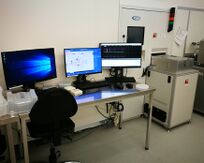
The DRIE-Pegasus 2 operator station and load lock in the DTU Nanolab cleanroom A-1. Photo: DTU Nanolab internal
|
The DRIE-Pegasus3 and DRIE-Pegasus4 operator station and cassette loading stations. Photo: DTU Nanolab internal
|
The Bosch process
The DRIE Pegasus tools are state-of-art silicon dry etchers that offer outstanding performance in terms of etch rate, uniformity etc. They use the so-called Bosch process to achieve excellent control of the etched features. Click HERE to access the top of the page. The contents are:
- Description of the Bosch process
- Processing options on the Pegasus
- Modification of the showerhead
- RF matching
- RF matching in general
- Why RF matching is extremely important in the Bosch process
- Picoscope process monitoring
As of 2017, completing the Dry Etch TPT course is mandatory for all new users. On the TPT web page you will find a version of the latest lecture slides - here you will find information as well.
Links to the individual pages for the Pegasi
Equipment performance and process related parameters
Process information
Process notation
Describing a process recipe on the Pegasus may sometimes be difficult because of the great flexibility of the instrument. A compact and precise notation is therefore required for the recipes. Click HERE to find a short description.
Hardware changes
A few hardware modifications have been made on the Pegasus 1 since it was installed in 2010. The changes are listed in the table below under hardware options.
General Pegasus information
Wafer bonding
To find information on how to bond wafers or chips to a carrier wafer, click HERE.
Characterisation of etched trenches
The trenches in deep silicon trenches can be characterized in many ways. Being able to compare processes requires that a set of common measurements and calculations must be established. Click HERE to find more information about the parameters used on the DRIE-Pegasus process development.


