[[image:Til LA forside 2024-05-03 161145.png|right|500x500px|thumb|Photos: DTU Nanolab]]
[[image:Til LA forside 2024-05-03 161145.png|right|500x500px|thumb|link=|Photos: DTU Nanolab]]
{{cc-nanolab}}
LabAdviser is a Wiki owned by DTU Nanolab for users of our facilities. It was created with the main purpose of sharing knowledge. It contains information about available equipment and fabrication processes in the cleanroom facilities in building 346/347 and the electron microscopes and supporting tools in 307/314.
LabAdviser is a Wiki for users of DTU Nanolab facilities created with the main puprose of sharing knowledge. It contains information about available equipment and fabrication processes in the cleanroom facilities in 346/347 and the characterisation equipment in building 307/314.
LabAdviser is designed to help you identify the right equipment and provide a solid starting point for your cleanroom processes or for further optimization to meet specific requirements. However, due to ongoing development of tools and processes, some information may be incomplete or not up-to-date. We make every effort to provide reliable information but we provide no warranty as to the accuracy, reliability or completeness of the information found in LabAdviser.
LabAdviser is designed to help you identify the right equipment and provide a solid starting point for your cleanroom processes or further optimization to meet specific requirements. However, due to ongoing development of tools and processes, some information may be incomplete or not up-to-date.
Please note that LabAdviser is not a replacement for direct communication with DTU Nanolab staff. We strongly recommend reviewing the information on LabAdviser as preparation before reaching out to staff members.
Please note that LabAdviser is not a replacement for direct communication with DTU Nanolab staff. We make every effort to provide reliable information but we provide no warranty as to the accuracy, reliability or completeness of the information found in LabAdviser. We strongly recommend reviewing the information on LabAdviser as preparation before reaching out to staff members.
If in doubt, you are always welcome to contact us via [mailto:nanolabsupport@nanolab.dtu.dk nanolabsupport@nanolab.dtu.dk].
If in doubt, you are always welcome to contact us via [mailto:nanolabsupport@nanolab.dtu.dk nanolabsupport@nanolab.dtu.dk].
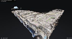
[[Image:Virtual tour in the clean room.JPG|right|300px|thumb|Take a virtual tour in the DTU Nanolab cleanroom [[https://www.nanolab.dtu.dk/capabilities/cleanroom-3d-tour]]]]
[[Image:Virtual tour in the clean room.JPG|right|300px|thumb|link=https://www.nanolab.dtu.dk/capabilities/cleanroom-3d-tour|Click to Enter the Virtual Tour through DTU Nanolabs cleanroom]]
<BR>Even if you are not a current user at our facilities, you are welcome to surf around. Please note that note that not all information might be available without login. You can take a [https://www.nanolab.dtu.dk/capabilities/cleanroom-3d-tour '''Virtual Tour of the DTU Nanolab cleanroom facility''']. Please also take a look at our homepage [https://www.nanolab.dtu.dk/english '''www.nanolab.dtu.dk'''] for more information on how to get access and/or collaborate with us as well as our capabilities and research.
<BR>Even if you are not a current user at our facilities, you are welcome to surf around. Please note that not all information is available without login. You can take a [https://www.nanolab.dtu.dk/capabilities/cleanroom-3d-tour Virtual Tour of the DTU Nanolab cleanroom facility]. Please also take a look at our homepage [https://www.nanolab.dtu.dk/english www.nanolab.dtu.dk] for more information on how to get access and/or collaborate with us as well as our capabilities and research.
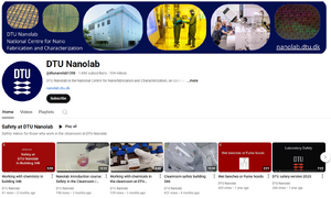
[[Image:YouTube.JPG|right|300px|thumb|DTU Nanolab on YouTube [[https://www.youtube.com/channel/UCJhdUTUJRDNODNiC3V95RQQ]]]]
[[Image:YouTube.JPG|right|300px|thumb|link=https://www.youtube.com/@dtunanolab1398|Click to Visit DTU Nanolab on YouTube ]]
You are also welcome to explore our [https://www.youtube.com/channel/UCJhdUTUJRDNODNiC3V95RQQ '''YouTube channel'''] with a selection of training videos.
You are also welcome to explore our [https://www.youtube.com/channel/UCJhdUTUJRDNODNiC3V95RQQ YouTube channel] with a selection of training videos.
<BR><BR><br>
<BR><BR><br>
'''LabAdviser contains information about'''
'''LabAdviser contains information about'''
*Equipment available in- and outside of the Cleanroom Facility (building 346)
*Equipment available in- and outside of the Cleanroom Facility (building 346)
*Equipment for Characterization, primarily Electron Microscopy (building 314 and 307)
*Equipment for Characterization, primarily Electron Microscopy (building 314 and 307)
*Equipment available in the PolyFabLab and PolySupLab (building 347)
*Equipment available in the PolyFabLab and SupportLab (building 347)
*Processes for Micro- and Nanofabrication available at DTU Nanolab
*Processes for Micro- and Nanofabrication available at DTU Nanolab
*Methods in Electron Microscopy available in building 314/307
*Methods in Electron Microscopy available in building 314/307
<br>
<br>
<br>
<br>
'''How Labadviser works'''
==How Labadviser works==
The structure of LabAdviser allows users to begin their search either from a known '''material''' or a known '''process'''. For example, if your process involves depositing a gold layer, you would start with the '''Thin Film Deposition''' section. There, you will find two tables, overview over relevant
Among others information, Labadviser offers users nano- and microfabrication information on how to build up a process flow, f.ex.
how to create a pattern, what materials to use, what process or equipment to use, how to avoid cross contamination between machines, or how to clean samples.
* Overview of relevant '''Materials''' organized in groups, such semiconductors, oxides, nitrides, metals, etc.
The structure of LabAdviser allows users to begin their search either from a known process. For example, if your process involves depositing a gold layer, you would start with the "Thin Film Deposition" section. There, you will find two tables:
* Available thin film '''Deposition Equipment'''
* Overview of '''Materials''', ''such semiconductors, oxides, nitrides, metals, etc.''
* Overview over '''Thin Film Deposition Equipment''', ''such as thermal evaporator, e-beam evaporator, sputter coater, etc.''
If you know the material you want to deposit but are unsure which tool to use or how different deposition methods compare, you can select the material (e.g. ''gold''). You will then be directed to a subpage listing all equipment capable of depositing that material and, if available, with some additional material-specific process information.
If you know the material you want to deposit but are unsure which tool to use or how different deposition methods compare, you can select the material (e.g. ''gold''). You will then be directed to a subpage listing all equipment capable of depositing that material and, if available, with some additional material-specific process information.
Line 39:
Line 40:
<br>
<br>
<br>
<br>
'''How to add Information to Labadviser'''
==How to add Information to Labadviser==
Sharing knowledge is the key for further development and all our users are encouraged to contribute. In our laboratories thousands of experiments are made. We want to make sure that the knowledge and experience acquired through these become accessible to current and future users. We are interested in any process development being done on our equipment, and even single tests of new recipes can be helpful. For the safety of our users as well as our equipment, we cannot allow LabAdviser to have an open-for-all-input structure like Wikipedia. Any feedback and/or input is welcome and can be send to the LabAdviser mailbox: [mailto:labadviser@nanolab.dtu.dk labadviser@nanolab.dtu.dk].
Sharing knowledge is the key for further development and all our users are encouraged to contribute. In our laboratories thousands of experiments are made. We want to make sure that the knowledge and experience acquired through these become accessible to current and future users. We are interested in any process development being done on our equipment, and even single tests of new recipes can be helpful. For the safety of our users as well as our equipment, we cannot allow LabAdviser to have an open-for-all-input structure like Wikipedia.
You will be credited for the material that you provide to us. We want to credit the right people for their work and be sure that we do not violate any rights or patents, etc. To publish your material in Labadviser we will ask you for a written permission to publish your work.
We are committed to giving proper credit to all contributors. If you provide material for publication in Labadviser, you will be clearly acknowledged as the author or source. Before publishing your material, we will request your written permission to do so. This ensures transparency and respect for your rights as a creator. More information regarding copyrights can be found [[LabAdviser:Copyright | <b>here</b>]].
Any feedback or input is welcome and can be send to the LabAdviser mailbox: [mailto:labadviser@nanolab.dtu.dk labadviser@nanolab.dtu.dk].
<br>
<br>
== Surveys and statistics ==
== Surveys and Statistics ==
'''Surveys'''
'''Surveys'''
Line 65:
Line 69:
[https://labmanager.dtu.dk/function.php?module=PeriodicDocument&view=docs&page_id=397 Tech Forum Slides]
[https://labmanager.dtu.dk/function.php?module=PeriodicDocument&view=docs&page_id=397 Tech Forum Slides]
== Contents ==
''this part is under construction'''
<!--*'''[[/Introduction to LabAdviser and Processing|Introduction to LabAdviser and Micro/Nano Fabrication]]'''
*'''[[Surveys and statistics|Surveys, statistics, monthly LabAdviser updates and other info.]]'''
!colspan="3" style="text-align:left;" | [[image:Create a film on your sample.png|x100px|Create a layer/film on your sample]] Create a layer/film on your sample
|-
!Entry page in LabAdviser
!Techniques
!Materials
|-
|[[Specific Process Knowledge/Thermal Process/Oxidation| Thermal Process/Oxidation]]
|Thermal oxidation
|Thermal SiO2
|-
|rowspan="8" valign="top"|[[Specific Process Knowledge/Thin film deposition| Thin film deposition]]
!colspan="3" style="text-align:left;" | [[image:Thermal treat your sample.png|x100px|Thermal treatment of your sample]] Thermal treatment of your sample
|-
!Entry page in LabAdviser
!Techniques
!Materials
|-
|rowspan="5" valign="top"|[[Specific Process Knowledge/Thermal Process|Thermal Process]]
|Annealing (>350C)
|Si, PECVD layers, Al, BCB curing, Polymer
|-
|Oxidation
|Si wafers
|-
|Doping with B/P
|Si wafers
|-
|Pyrolysis
|Resists: AZ, SU8, PDMS
|-
|Rapid Thermal Anneal (RTP)
|SiO2, Si3N4, Ti, III-V
|-
|
[[Specific Process Knowledge/Lithography/Baking| Lithography/Baking]] <br>
!colspan="3" style="text-align:left;" | [[image:Transfer mask pattrn to your sample.png|x100px|Transfer mask pattern to your sample]] Transfer mask pattern to your sample
|-
!Entry page in LabAdviser
!Techniques
!Materials
|-
|rowspan="2" valign="top"|[[Specific Process Knowledge/Etch| Etch]]
!colspan="3" style="text-align:left;" | [[image:Define your structure directly.png|x100px|Define the structure directly on your sample]] Define your structure directly
|-
!Entry page in LabAdviser
!Techniques
!Materials
|-
|rowspan="5" valign="top"|[[Specific Process Knowledge/Direct Structure Definition|Direct Structure Definition]]
| style="background:WhiteSmoke; color:black" | All requests regarding equipment training and process flows. Please add your Name to the subject line.<BR><BR> <i>Note: Requests are commonly answered within 2 workdays. </i>
|-
|-
| style="background: LightGrey; color:black" | '''E-beam training'''
| align="center" style="background: LightGrey; color:black" | [mailto:e-beam@nanolab.dtu.dk e-beam@nanolab.dtu.dk]
| style="background: LightGrey; color:black" | Requests regarding training on JEOL JBX-9500FSZ or Raith Eline e-beam systems. Please study the material on [[Specific Process Knowledge/Lithography/EBeamLithography|the EBL Labadviser pages]] beforehand.
| style="background: LightGrey; color:black" | '''General inquiries'''
| align="center" style="background: LightGrey; color:black" | [mailto:nanolabsupport@nanolab.dtu.dk?subject=⟨user%20name⟩%20⟨subject⟩ nanolabsupport@nanolab.dtu.dk]
| style="background: LightGrey; color:black" | Inquiries related to machines, cleanroom access, Mask review, tool changes, and others. Please add your Name to the subject line. <BR><BR> <i>Note: Requests are commonly answered within 2 workdays. </i>
| style="background:WhiteSmoke; color:black" | Requests for change of metal in Thin Film Deposition equipment. <BR> See current and future materials in statuslog of the respective machines.
<BR>
[http://labmanager.dtu.dk/function.php?module=Machine&view=log&mach=244&type=status Lesker - status log]
<BR>
[http://labmanager.dtu.dk/function.php?module=Machine&view=log&mach=429&type=status E-Beam Evaporator (Temescal) - status log]
<BR>
[https://labmanager.dtu.dk/function.php?module=Machine&view=log&mach=511&type=status E-Beam Evaporator (10-pockets) - status log]
<BR>
[https://labmanager.dtu.dk/function.php?module=Machine&view=log&mach=441&type=status Sputter-System Metal-Oxide(PC1) - status log]
LabAdviser is a Wiki owned by DTU Nanolab for users of our facilities. It was created with the main purpose of sharing knowledge. It contains information about available equipment and fabrication processes in the cleanroom facilities in building 346/347 and the electron microscopes and supporting tools in 307/314.
LabAdviser is designed to help you identify the right equipment and provide a solid starting point for your cleanroom processes or for further optimization to meet specific requirements. However, due to ongoing development of tools and processes, some information may be incomplete or not up-to-date. We make every effort to provide reliable information but we provide no warranty as to the accuracy, reliability or completeness of the information found in LabAdviser.
Please note that LabAdviser is not a replacement for direct communication with DTU Nanolab staff. We strongly recommend reviewing the information on LabAdviser as preparation before reaching out to staff members.
Click to Enter the Virtual Tour through DTU Nanolabs cleanroom
Even if you are not a current user at our facilities, you are welcome to surf around. Please note that not all information is available without login. You can take a Virtual Tour of the DTU Nanolab cleanroom facility. Please also take a look at our homepage www.nanolab.dtu.dk for more information on how to get access and/or collaborate with us as well as our capabilities and research.
Click to Visit DTU Nanolab on YouTube
You are also welcome to explore our YouTube channel with a selection of training videos.
LabAdviser contains information about
Equipment available in- and outside of the Cleanroom Facility (building 346)
Equipment for Characterization, primarily Electron Microscopy (building 314 and 307)
Equipment available in the PolyFabLab and SupportLab (building 347)
Processes for Micro- and Nanofabrication available at DTU Nanolab
Methods in Electron Microscopy available in building 314/307
How Labadviser works
Among others information, Labadviser offers users nano- and microfabrication information on how to build up a process flow, f.ex.
how to create a pattern, what materials to use, what process or equipment to use, how to avoid cross contamination between machines, or how to clean samples.
The structure of LabAdviser allows users to begin their search either from a known process. For example, if your process involves depositing a gold layer, you would start with the "Thin Film Deposition" section. There, you will find two tables:
Overview of Materials, such semiconductors, oxides, nitrides, metals, etc.
Overview over Thin Film Deposition Equipment, such as thermal evaporator, e-beam evaporator, sputter coater, etc.
If you know the material you want to deposit but are unsure which tool to use or how different deposition methods compare, you can select the material (e.g. gold). You will then be directed to a subpage listing all equipment capable of depositing that material and, if available, with some additional material-specific process information.
Alternatively, if you're more interested in a specific piece of equipment, or wish to explore which materials it can process, selecting that equipment will lead you to a dedicated page with detailed process information, including compatible materials.
How to add Information to Labadviser
Sharing knowledge is the key for further development and all our users are encouraged to contribute. In our laboratories thousands of experiments are made. We want to make sure that the knowledge and experience acquired through these become accessible to current and future users. We are interested in any process development being done on our equipment, and even single tests of new recipes can be helpful. For the safety of our users as well as our equipment, we cannot allow LabAdviser to have an open-for-all-input structure like Wikipedia.
We are committed to giving proper credit to all contributors. If you provide material for publication in Labadviser, you will be clearly acknowledged as the author or source. Before publishing your material, we will request your written permission to do so. This ensures transparency and respect for your rights as a creator. More information regarding copyrights can be found here.
Any feedback or input is welcome and can be send to the LabAdviser mailbox: labadviser@nanolab.dtu.dk.
Surveys and Statistics
Surveys
DTU Nanolab performs regular customer surveys which are available on LabManager. Access to LabManager requires a DTU account and access to DTU Nanolab facilities.
The purpose of the Nanolab Technology Forum is to discuss the current and future technological possibilities at Nanolab, including user requirements, current equipment status, equipment acquisition, funding, etc.
Tech Forum slides are available on LabManager. Access to LabManager requires a DTU account and access to DTU Nanolab facilities.