Specific Process Knowledge/Lithography/EBeamLithography/JEOLPatternPreparation: Difference between revisions
| (45 intermediate revisions by one other user not shown) | |||
| Line 1: | Line 1: | ||
'''Feedback to this page''': '''[mailto:labadviser@nanolab.dtu.dk?Subject=Feed%20back%20from%20page%20http://labadviser.nanolab.dtu.dk/index.php/Specific_Process_Knowledge/Lithography/EBeamLithography click here]''' | '''Feedback to this page''': '''[mailto:labadviser@nanolab.dtu.dk?Subject=Feed%20back%20from%20page%20http://labadviser.nanolab.dtu.dk/index.php/Specific_Process_Knowledge/Lithography/EBeamLithography click here]''' | ||
Content and illustration by Thomas Pedersen | Content and illustration by Thomas Pedersen, DTU Nanolab unless otherwise noted. | ||
=Pattern preparation for exposure on JEOL 9500 = | =Pattern preparation for exposure on JEOL 9500 = | ||
Prior to exposure a pattern must be prepared for exposure. The original pattern must be provided in GDS format. Depending on requirements and complexity level pattern preparation will involve all or subset of the following steps. | Prior to exposure a pattern must be prepared for exposure. The original pattern must be provided in GDS format. Depending on requirements and complexity level pattern preparation will involve all or subset of the following steps. | ||
*Exposure time estimation | |||
*Placement preparation | *Placement preparation | ||
*Alignment preparation | *Alignment preparation | ||
| Line 14: | Line 15: | ||
Some steps are done using Beamer from GenISys GmbH. We advise all users to familiarise themselves with Beamer [https://www.genisys-gmbh.com/webinar-series-beamer-training.html through the tutorial series found on GenISys own website.] or from our own [[Specific_Process_Knowledge/Lithography/EBeamLithography/BEAMER|Beamer guide.]] | Some steps are done using Beamer from GenISys GmbH. We advise all users to familiarise themselves with Beamer [https://www.genisys-gmbh.com/webinar-series-beamer-training.html through the tutorial series found on GenISys own website.] or from our own [[Specific_Process_Knowledge/Lithography/EBeamLithography/BEAMER|Beamer guide.]] | ||
Please observe that wafers are clamped in such a way that it is not possible to expose the rim of the wafer. The patternable diameter for wafers are as listed below. Writing a pattern outside this area does not damage the tool but it is a waste of time. | |||
*2": 44 mm | |||
*4": 93 mm | |||
*6": 138 mm | |||
<br> | |||
== | ==Exposure time estimation== | ||
=== Boundary box | The writing time should always be estimated prior to an exposure session. The writing time ''t'' [s] is a function of exposure dose ''Q'' [C/cm<sup>2</sup>], pattern area ''A'' [m<sup>2</sup>] and beam current ''I'' [A], can calculated as | ||
In continuation of the example above, if two layers | |||
''t = QA/I'' | |||
As a rule of thumb and easy extrapolation, exposure of an area of 1.000.000 µm<sup>2</sup> at 1 nA and exposure dose of 100 µC/cm<sup>2</sup> takes 17 min. A simple Excel sheet to estimate writing time is [[:File:WritingTimeEstimator.xlsx|available here.]] The area can in principle be obtained from the design layout program, some layout programs are however surprisingly poor at giving a correct total area unless the design is very simple. In general the best way to obtain the total area is by importing the design into Beamer and reading the area from the import log or the pattern viewer. | |||
<br> | |||
== Pattern placement == | |||
Pattern placement on the JEOL system has a very important difference regarding patttern placement compared to our Heidelberg MLA systems. Pattern placement is entirely dependent on the boundary box of the design. The boundary box is simply defined as the smallest box enclosing the entire design. All patterns are placed using the '''ARRAY''' command and they are placed with respect to the '''center of the design boundary box.''' This is illustrated below with the two designs, L1 and L2. L1 is a design nicely centered around (0,0) with a symmetric bounding box. When placed by the '''ARRAY''' command at (0,0) this will come out entirely as expected. L2 does however not have a bounding box centered around (0,0) and when placed by the '''ARRAY''' command at (0,0), it will be exposed at the center of the substrate. Thus, it is vital to keep the bounding box in mind as the '''ARRAY command places patterns with respect to the center of the bounding box.''' This is in stark contrast to how the MLA UV lithography systems work and it is often essential to intentionally control the bounding box of a pattern. | |||
{| style="border: none; border-spacing: 0; margin: 1em auto; text-align: center;" | |||
|- | |||
| [[image:BoundingBox.png|1000px]] | |||
|- | |||
| colspan="1" style="text-align:center;| | |||
Illustration of the importance of the bounding box of a pattern. Patterns are always placed with respect to the center of their bounding box. | |||
|} | |||
=== Boundary box control === | |||
In continuation of the example above, if two layers are to be positioned correctly relative to each other it is vital to control the extend of the boundary box, since '''the ARRAY command places patterns with respect to the center of the bounding box'''. In the example above the bounding box of L2 is not symmetric around the design coordinate system (0,0) and hence it will be moved to the substrate center during exposure, unless the user defines an offset in the '''ARRAY''' command that places the pattern. | |||
The bounding box of L2 can be controlled in two ways: | |||
*Letting L2 inherit the L1 boundary box (option in Beamer) | *Letting L2 inherit the L1 boundary box (option in Beamer) | ||
*Placing small corner marks on L2 to force the boundary box as needed | *Placing small corner marks on L2 to force the boundary box as needed | ||
Corner marks can be 1x1 nm boxes placed | In the example below corner marks are placed symmetric around design system (0,0) on L2 and hence the bounding box of L2 is now symmetric around design (0,0). Corner marks can be 1x1 nm boxes, hencce they will be too small to actually show up in the developed resist pattern. | ||
{| style="border: none; border-spacing: 0; margin: 1em auto; text-align: center;" | |||
|- | |||
| [[image:BoundingBoxAlign.png|1000px]] | |||
|- | |||
| colspan="1" style="text-align:center;| | |||
Illustration of bounding box control by intentionally adding control geometry to force the bounding box to be symmetric around design system (0,0) on L2. | |||
|} | |||
== Alignment preparation == | |||
Alignment on the JEOL 9500 system has a few quirks and pitfalls as a few key elements are not immediately intuitive. The first step to a succesful alignment is proper pattern preparation and understanding how patterns are placed by the system. | |||
===Wafer scale and chip array alignment=== | |||
There is two fundamentally different approaches to pattern alignment on the JEOL 9500 system. One can either do a wafer scale layout where essentially one design covering all elements of the pattern is exposed, i.e. a 1 by 1 array as defined by the ARRAY command. Or, one can expose chips instanced into an array using the ARRAY command. In the first case the pattern can only be aligned via global alignment to a single set of alignment marks defining the wafer coordinate system. In the second case, an initial wafer alignment is made but each chip can then be individually aligned to an extra set of individual chip alignment marks. This is illustrated below. | |||
In the wafer scale layout, L1 is exposed with a set of global alignment marks (P & Q marks) in order to allow alignment of the next wafer scale layer, L2. Thus the placement of L2 is determined entirely by a single set of alignment marks. In the chip array design, in addition to the global alignment marks (P & Q marks) chip alignment marks for each instance of the chip design is also produced. Thus the placement of each instance of L2 is determined by a local mark very close to where the pattern of L2 is actually printed for increased alignment precision. | |||
Global alignment using P & Q marks is done using the SETWFR subprogram. The P & Q mark coordinates are defined in the substrate coordinate system (X,Y). For instance, on a 4" wafer it is typical to place the P and Q marks at (-35000,0) and (35000,0), respectively. | |||
Chip marks are different however as illustrated in the right most part of the illustration below. Chip mark coordinates refer to the local chip coordinate system (X',Y'). For instance, if a chip design has a size of 800 x 800 µm it would be convenient to place chip alignment marks at M1 = (-500,500), M2 = (500,500), M3 = (500,-500) and M4 = (-500,-500). If using more than one chip mark the order must be as specified in the illustration. The JEOL system supports 1 or 4 mark chip alignment (CHIPAL 1 or CHIPAL 4). | |||
[[ | {| style="border: none; border-spacing: 0; margin: 1em auto; text-align: center;" | ||
|- | |||
| [[image:EBL_align.png|1000px]] | |||
|- | |||
| colspan="1" style="text-align:center;| | |||
Illustration of wafer scale pattern alignment and chip array alignment for two designs, L1 and L2. | |||
|} | |||
=== Detection of alignment mark === | === Detection of alignment mark === | ||
If alignment is needed it is vital to consider this already at the process design and mask design level to ensure that a visible mark is produced. Alignment is done using the electron beam in either SEM mode or beam scan mode. In SEM mode the stage is moved to the expected alignment mark position and the user will manually observe the SEM image and adjust stage position to center the mark at as high magnification as required by alignment tolerance of the design. In beam scan mode the user sets up a routine that will scan the beam across the expected mark position and the Backscatter Electron Detector (BED) will detect the backscattered signal. This is done in both x- and y-directions and system will calculate the mark center based on | If alignment is needed it is vital to consider this already at the process design and mask design level to ensure that a visible mark is produced. Alignment is done using the electron beam in either SEM mode or beam scan mode. It is vital that the mark produced is visible in a 100 kV SEM or from a 100 kV beam scan. For this purpose marks made by heavy metals or etched trences with an aspect rate of at least 1 is preferable. In SEM mode the stage is moved to the expected alignment mark position and the user will manually observe the SEM image and adjust stage position to center the mark at as high magnification as required by alignment tolerance of the design. In beam scan mode the user sets up a routine that will scan the beam across the expected mark position and the Backscatter Electron Detector (BED) will detect the backscattered signal. This is done in both x- and y-directions and the system will calculate the mark center based on the second derivative of the backscatter signal. | ||
[[ | {| style="border: none; border-spacing: 0; margin: 1em auto; text-align: center;" | ||
|- | |||
| [[image:JEOL9500Alignment.png|800px]] | |||
|- | |||
| colspan="1" style="text-align:center;| | |||
Illustration of SEM mode alignment and beam scan alignment. | |||
|} | |||
The advantage of SEM mode is that it is fairly straight forward to do. It is however also very slow as it requires constant user input to move the stage at higher and higher magnification levels until position is sufficiently determined. Due to the time it takes it is hardly realistic to do chip alignment, only global wafer alignment should be done in this way. | The advantage of SEM mode is that it is fairly straight forward to do. It is however also very slow as it requires constant user input to move the stage at higher and higher magnification levels until position is sufficiently determined. Due to the time it takes it is hardly realistic to do chip alignment, only global wafer alignment should be done in this way. | ||
| Line 60: | Line 117: | ||
[[File:9500MarkScan4.png|800px|center|frameless]] | [[File:9500MarkScan4.png|800px|center|frameless]] | ||
==Fracturing== | |||
Pattern fracturing is an essential part of the pattern preparation process. Pattern fracturing will automatically happen at either Proximity Effect Correction in Beamer or upon export to V30. If one does not actively change fracturing parameters it will be done with default parameters which can work great in many cases. For best possible result it can however be necessary to actively control how the pattern is fractured, how beam shots are placed to form the pattern and what order pattern elements are written in. This can all be controlled with the ''Fracture'' node in Beamer and hence in combination with the ''PEC'' node it is one of the most impactful nodes. In this section we will illustrate some of the issues that the ''Fracture'' node can help mitigate. For information on the ''Fracture'' node in Beamer, please refer to the Beamer guide. | |||
For precise control of critical dimension (CD) for small features it is important to consider the actual beam size and how it is placed, i.e. how the shapes are filled with beam shots. This is illustrated in the three shapes below. The left shape is 25 x 25 nm and written with a 5 nm beam spot. This works very well. However, if one wishes to write a 28 x 28 nm shape under the same circumstances shot filling becomes an issue. Similarly in the right hand shape, any shape that has a sloped edge will have shot filling issues. It is obvious that these issues are only a concern when CD control on a sub beam size level is needed. | |||
{| style="border: none; border-spacing: 0; margin: 1em auto; text-align: center;" | |||
|- | |||
| [[image:ShotFilling.png|800px]] | |||
|- | |||
| colspan="1" style="text-align:center;| | |||
Illustration of shot filling issues for small shapes. | |||
|} | |||
== Bulk and sleeve separation - double current exposure == | == Bulk and sleeve separation - double current exposure == | ||
Patterns that contain a mix of fine and large dimension structures can advantageously be broken into a low current and a high current exposure. In this way the fine features can be written at low current (and low speed) and the large structures can be written at high current (and high speed). Some patterns, for instance a fine electrode pattern with large bonding pads, can easily and manually be broken into a fine and coarse part and placed in two different layers. For many patterns this can however be very cumbersome but the process can also be automated with Beamer using "bulk and sleeve" setup. The concept is illustrated below. In this setup, Beamer will extract the periphery (sleeve) of a pattern into one layer and the bulk of structures into another layer. The bulk is oversized slightly (adding a bias) to ensure overlap between the two patterns at exposure. In this way structures can be defined with best possible edge definition while keeping exposure time down. [https://labmanager.dtu.dk/view_binary.php?fileId=5412 A Beamer flow with a default bulk and sleeve setup can be found here.] A | Patterns that contain a mix of fine and large dimension structures can advantageously be broken into a low current and a high current exposure. In this way the fine features can be written at low current (and low speed) and the large structures can be written at high current (and high speed). Some patterns, for instance a fine electrode pattern with large bonding pads, can easily and manually be broken into a fine and coarse part and placed in two different layers. For many patterns this can however be very cumbersome but the process can also be automated with Beamer using "bulk and sleeve" setup. The concept is illustrated below. In this setup, Beamer will extract the periphery (sleeve) of a pattern into one layer and the bulk of structures into another layer. The bulk is oversized slightly (adding a bias) to ensure overlap between the two patterns at exposure. In this way structures can be defined with best possible edge definition while keeping exposure time down. [https://labmanager.dtu.dk/view_binary.php?fileId=5412 A Beamer flow with a default bulk and sleeve setup can be found here.] A 500 nm sleeve with a 200 nm overlap is a good starting point. | ||
| Line 87: | Line 158: | ||
*Use a nummerical PSF | *Use a nummerical PSF | ||
The pre-computed PSF can be loaded from either a separate file, from the local archive or from the global archive. In any case the file will probably originate from a Tracer simulation | The pre-computed PSF can be loaded from either a separate file, from the local archive or from the global archive. In any case the file will probably originate from a Tracer simulation. It can be advantageus to place your PSF in the global (network) archive such that it is available on the Beamer PC in the cleanroom as well as the Beamer PC outside the cleanroom. | ||
A guassian approximation is mostly useful if trying to replicate a result from litterature or if one has worked deliberately towards determining the gaussian constants for a particular process. | A guassian approximation is mostly useful if trying to replicate a result from litterature or if one has worked deliberately towards determining the gaussian constants for a particular process. | ||
Latest revision as of 14:07, 17 September 2025
Feedback to this page: click here
Content and illustration by Thomas Pedersen, DTU Nanolab unless otherwise noted.
Pattern preparation for exposure on JEOL 9500
Prior to exposure a pattern must be prepared for exposure. The original pattern must be provided in GDS format. Depending on requirements and complexity level pattern preparation will involve all or subset of the following steps.
- Exposure time estimation
- Placement preparation
- Alignment preparation
- Bulk and sleeve separation
- Proximity Effect Correction
- Export to V30
Some steps are done using Beamer from GenISys GmbH. We advise all users to familiarise themselves with Beamer through the tutorial series found on GenISys own website. or from our own Beamer guide.
Please observe that wafers are clamped in such a way that it is not possible to expose the rim of the wafer. The patternable diameter for wafers are as listed below. Writing a pattern outside this area does not damage the tool but it is a waste of time.
- 2": 44 mm
- 4": 93 mm
- 6": 138 mm
Exposure time estimation
The writing time should always be estimated prior to an exposure session. The writing time t [s] is a function of exposure dose Q [C/cm2], pattern area A [m2] and beam current I [A], can calculated as
t = QA/I
As a rule of thumb and easy extrapolation, exposure of an area of 1.000.000 µm2 at 1 nA and exposure dose of 100 µC/cm2 takes 17 min. A simple Excel sheet to estimate writing time is available here. The area can in principle be obtained from the design layout program, some layout programs are however surprisingly poor at giving a correct total area unless the design is very simple. In general the best way to obtain the total area is by importing the design into Beamer and reading the area from the import log or the pattern viewer.
Pattern placement
Pattern placement on the JEOL system has a very important difference regarding patttern placement compared to our Heidelberg MLA systems. Pattern placement is entirely dependent on the boundary box of the design. The boundary box is simply defined as the smallest box enclosing the entire design. All patterns are placed using the ARRAY command and they are placed with respect to the center of the design boundary box. This is illustrated below with the two designs, L1 and L2. L1 is a design nicely centered around (0,0) with a symmetric bounding box. When placed by the ARRAY command at (0,0) this will come out entirely as expected. L2 does however not have a bounding box centered around (0,0) and when placed by the ARRAY command at (0,0), it will be exposed at the center of the substrate. Thus, it is vital to keep the bounding box in mind as the ARRAY command places patterns with respect to the center of the bounding box. This is in stark contrast to how the MLA UV lithography systems work and it is often essential to intentionally control the bounding box of a pattern.

|
|
Illustration of the importance of the bounding box of a pattern. Patterns are always placed with respect to the center of their bounding box. |
Boundary box control
In continuation of the example above, if two layers are to be positioned correctly relative to each other it is vital to control the extend of the boundary box, since the ARRAY command places patterns with respect to the center of the bounding box. In the example above the bounding box of L2 is not symmetric around the design coordinate system (0,0) and hence it will be moved to the substrate center during exposure, unless the user defines an offset in the ARRAY command that places the pattern.
The bounding box of L2 can be controlled in two ways:
- Letting L2 inherit the L1 boundary box (option in Beamer)
- Placing small corner marks on L2 to force the boundary box as needed
In the example below corner marks are placed symmetric around design system (0,0) on L2 and hence the bounding box of L2 is now symmetric around design (0,0). Corner marks can be 1x1 nm boxes, hencce they will be too small to actually show up in the developed resist pattern.

|
|
Illustration of bounding box control by intentionally adding control geometry to force the bounding box to be symmetric around design system (0,0) on L2. |
Alignment preparation
Alignment on the JEOL 9500 system has a few quirks and pitfalls as a few key elements are not immediately intuitive. The first step to a succesful alignment is proper pattern preparation and understanding how patterns are placed by the system.
Wafer scale and chip array alignment
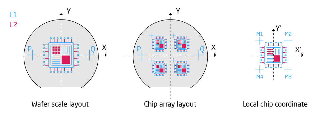
There is two fundamentally different approaches to pattern alignment on the JEOL 9500 system. One can either do a wafer scale layout where essentially one design covering all elements of the pattern is exposed, i.e. a 1 by 1 array as defined by the ARRAY command. Or, one can expose chips instanced into an array using the ARRAY command. In the first case the pattern can only be aligned via global alignment to a single set of alignment marks defining the wafer coordinate system. In the second case, an initial wafer alignment is made but each chip can then be individually aligned to an extra set of individual chip alignment marks. This is illustrated below.
In the wafer scale layout, L1 is exposed with a set of global alignment marks (P & Q marks) in order to allow alignment of the next wafer scale layer, L2. Thus the placement of L2 is determined entirely by a single set of alignment marks. In the chip array design, in addition to the global alignment marks (P & Q marks) chip alignment marks for each instance of the chip design is also produced. Thus the placement of each instance of L2 is determined by a local mark very close to where the pattern of L2 is actually printed for increased alignment precision.
Global alignment using P & Q marks is done using the SETWFR subprogram. The P & Q mark coordinates are defined in the substrate coordinate system (X,Y). For instance, on a 4" wafer it is typical to place the P and Q marks at (-35000,0) and (35000,0), respectively.
Chip marks are different however as illustrated in the right most part of the illustration below. Chip mark coordinates refer to the local chip coordinate system (X',Y'). For instance, if a chip design has a size of 800 x 800 µm it would be convenient to place chip alignment marks at M1 = (-500,500), M2 = (500,500), M3 = (500,-500) and M4 = (-500,-500). If using more than one chip mark the order must be as specified in the illustration. The JEOL system supports 1 or 4 mark chip alignment (CHIPAL 1 or CHIPAL 4).
|
|
Illustration of wafer scale pattern alignment and chip array alignment for two designs, L1 and L2. |
Detection of alignment mark
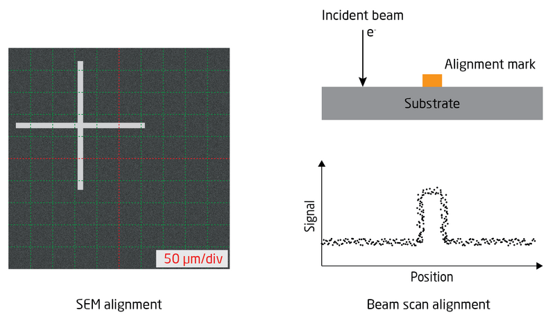
If alignment is needed it is vital to consider this already at the process design and mask design level to ensure that a visible mark is produced. Alignment is done using the electron beam in either SEM mode or beam scan mode. It is vital that the mark produced is visible in a 100 kV SEM or from a 100 kV beam scan. For this purpose marks made by heavy metals or etched trences with an aspect rate of at least 1 is preferable. In SEM mode the stage is moved to the expected alignment mark position and the user will manually observe the SEM image and adjust stage position to center the mark at as high magnification as required by alignment tolerance of the design. In beam scan mode the user sets up a routine that will scan the beam across the expected mark position and the Backscatter Electron Detector (BED) will detect the backscattered signal. This is done in both x- and y-directions and the system will calculate the mark center based on the second derivative of the backscatter signal.
|
|
Illustration of SEM mode alignment and beam scan alignment. |
The advantage of SEM mode is that it is fairly straight forward to do. It is however also very slow as it requires constant user input to move the stage at higher and higher magnification levels until position is sufficiently determined. Due to the time it takes it is hardly realistic to do chip alignment, only global wafer alignment should be done in this way.
Automatic alignment by beam scan is significantly faster, it only takes a couple of seconds per scan. Hence this is the only realistic way of doing chip alignment. It can however be challenging to get sufficient signal on the BED for this to work if this has not already been thought into the mask and process design. Bear in mind that the electron beam is 100 kV and unless there is a relatively high difference in atomic mass between mark and substrate the signal or contrast between substrate and mark will be too low. Gold marks on Si substrates will usually work great. Deep and narrow features etched into a substrate will also work fine. Please consult with the E-beam staff or experienced colleagues when making your mark design.
Design of global marks and chip marks
As a minimum two global alignment marks must be present on the substrate for alignment. In JEOL terms these are P and Q marks. These can be used to align a full substrate design or as initial alignment of chip arrays with individual chip marks. For chip alignment either one mark (M1) or four marks (M1-M4) must be used.

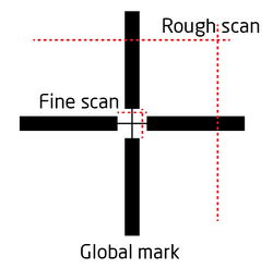
Global alignment (SETWFR) has a rough scan and a fine scan setting. Initially the mark is found using the rough scan setting, which is set to scan a long distance, typically 500 µm. Once the mark is located the machine will continue with the fine scan setting which will tyipcally scan <6 µm. In order for the machine to detect the mark on the rough scan setting the cross must have sufficient width and hence the cross is typically divided into a wide part and a slim part in the center. It is recommendable to use global marks of up to 1000 µm in height and width to make them easy and fast to find.
Chip marks are only scanned after a global alignment and hence the chip mark positions are usually very well known and the chip marks can be much smaller as indicated above.
Do NOT place any sort of text or other structures inside alignment crosses. If any other feature appear in a beam scan the system will not be able to determine which feature is the actual alignment cross.
Placement of alignment marks
Global alignment marks should be placed at the left-most and right-most part of the layout. They should however not be placed closer than 15 mm to the edge of a round wafer slot as this can interfere with height sensing of the alignment mark. If alignment marks are placed too close to the edge of a wafer slot height sensing of the marks must be disabled using the HSWITCH command.
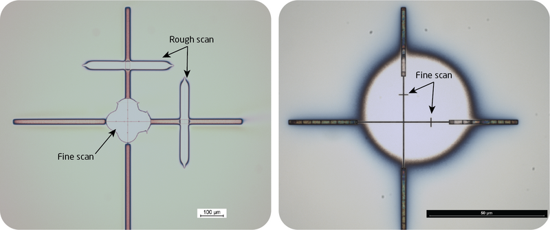
Chip marks should be placed at the corners of each chip with a gap of at least 100 µm to any important structure. Bear in mind that beam scan during alignment is a high dose exposure of the mark area and hence this resist will develop (for a positive resist). Eventhough the beam is only a few nm in diameter (dependent on exposure current) the affected area is much larger due to backscatter and proximity effect. This is illustrated in the microscope images below. On the left side is a global mark which has been scanned once in x and y rough scan and several times in fine scan mode at various locations. On the right is a chip mark that has been scanned a single time in x and y. It is obvious that the affected resist area is much larger than the scan area itself.
Fracturing
Pattern fracturing is an essential part of the pattern preparation process. Pattern fracturing will automatically happen at either Proximity Effect Correction in Beamer or upon export to V30. If one does not actively change fracturing parameters it will be done with default parameters which can work great in many cases. For best possible result it can however be necessary to actively control how the pattern is fractured, how beam shots are placed to form the pattern and what order pattern elements are written in. This can all be controlled with the Fracture node in Beamer and hence in combination with the PEC node it is one of the most impactful nodes. In this section we will illustrate some of the issues that the Fracture node can help mitigate. For information on the Fracture node in Beamer, please refer to the Beamer guide.
For precise control of critical dimension (CD) for small features it is important to consider the actual beam size and how it is placed, i.e. how the shapes are filled with beam shots. This is illustrated in the three shapes below. The left shape is 25 x 25 nm and written with a 5 nm beam spot. This works very well. However, if one wishes to write a 28 x 28 nm shape under the same circumstances shot filling becomes an issue. Similarly in the right hand shape, any shape that has a sloped edge will have shot filling issues. It is obvious that these issues are only a concern when CD control on a sub beam size level is needed.

|
|
Illustration of shot filling issues for small shapes. |
Bulk and sleeve separation - double current exposure
Patterns that contain a mix of fine and large dimension structures can advantageously be broken into a low current and a high current exposure. In this way the fine features can be written at low current (and low speed) and the large structures can be written at high current (and high speed). Some patterns, for instance a fine electrode pattern with large bonding pads, can easily and manually be broken into a fine and coarse part and placed in two different layers. For many patterns this can however be very cumbersome but the process can also be automated with Beamer using "bulk and sleeve" setup. The concept is illustrated below. In this setup, Beamer will extract the periphery (sleeve) of a pattern into one layer and the bulk of structures into another layer. The bulk is oversized slightly (adding a bias) to ensure overlap between the two patterns at exposure. In this way structures can be defined with best possible edge definition while keeping exposure time down. A Beamer flow with a default bulk and sleeve setup can be found here. A 500 nm sleeve with a 200 nm overlap is a good starting point.

Proximity Effect Correction (PEC)
Background information
Proximity Effect Correction (or Proximity Error Correction) is a huge topic in EBL and here we will demonstrate the simplest way to apply PEC to your pattern using Beamer. For further information and more advanced uses of Beamer we advise users to go through the tutorials on GenISys own website.
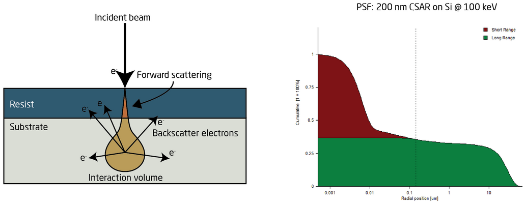
The proximity effect comes from backscattered electrons that will provide a secondary exposure to the resist, as illustrated below. Thus the exposure dose received by the resist has two components; the intentional exposure from the incident beam and an undesireable exposure from backscaterred electrons. The distance of which this secondary exposure will occur is dependent on substrate material and acceleration voltage. For silicon substrates exposed at 100 kV, the distance is up to 30 µm. The amount of secondary exposure will be pattern dependent since densely populated pattern areas will suffer a lot of secondary exposure while sparsely populated areas will not suffer much secondary exposure. This will cause a local pattern bias that will depend on local pattern load. In order to circumvent this one can modulate the incident dose to account for the proximity effect. The dose modulation can be calculated with Beamer. Beamer will essentially break the design into a number of dose classes and assign each a unique dose dependent on pattern density and feature dimension.
PEC is calculated based on a Point Spread Function (PSF). The PSF is a model of the radial energy distribution when taking backscatter electrons into account. In Beamer the PSF will look similar to the plot below that shows the cummulative radial energy PSF for a silicon substrate covered byt 200 nm resist exposed at 100 kV. Notice that the x-axis is logarithmic and in this case extends to about 30 µm from the center of the beam. The red part of the curve indicates beam spread due to forward scattering through the resist.
The PEC node in Beamer
Beamer provides three methods of defining a PSF:
- Load a pre-computer PSF from the archives
- Use a guassian approximation and enter the variables values
- Use a nummerical PSF
The pre-computed PSF can be loaded from either a separate file, from the local archive or from the global archive. In any case the file will probably originate from a Tracer simulation. It can be advantageus to place your PSF in the global (network) archive such that it is available on the Beamer PC in the cleanroom as well as the Beamer PC outside the cleanroom.
A guassian approximation is mostly useful if trying to replicate a result from litterature or if one has worked deliberately towards determining the gaussian constants for a particular process.
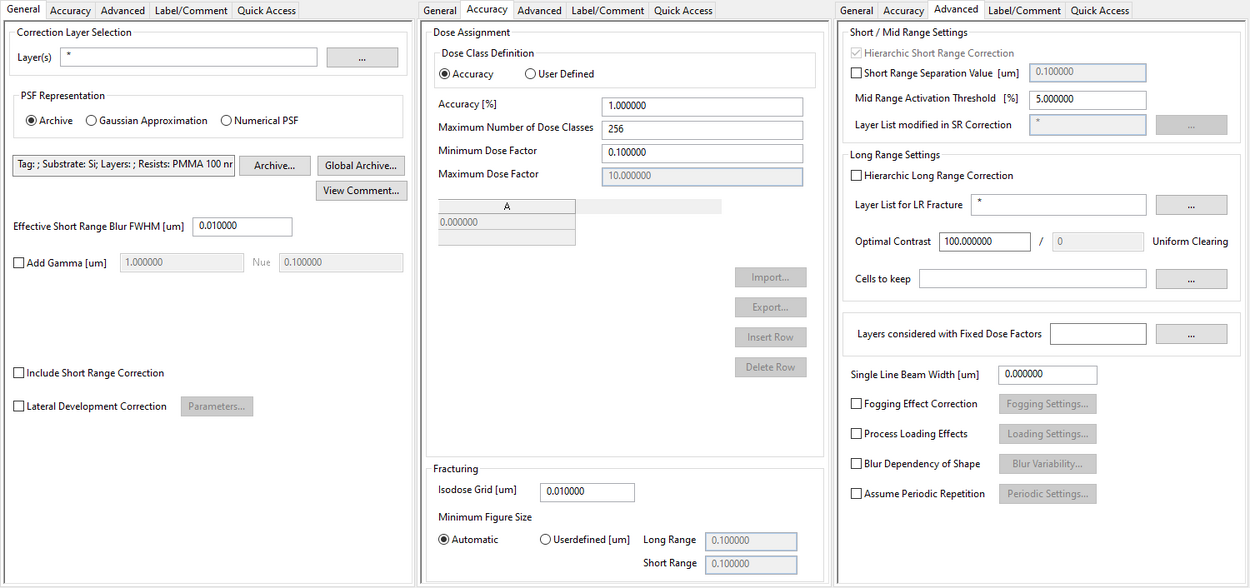
As seen above the PEC node has a lot of variables, more information can be found in the tutorials on the GenISys website, here we will only go through the most important options.
From the General tab the layer(s) to perform PEC can be selected through the Layer(s) field. The type of PSF is defined from the PSF Representation. Archived PSF's can be loaded from either the local machine Archive... or from the Global Archive... (network based and thus available on both Beamer computers). Forward scatter through the resist layer is disabled by default, it can be enabled with Include Short Range Correction at the expense of (sometimes a lot) extra computation time. Known development bias can be adjusted for in Lateral Development Correction.
In the Accuracy tab one can control the accuracy and element size of fractured elements. The Accuracy [%] field defines the maximum allowable difference in dose classes and thus has an impact on the number of dose classes generated. The Maximum Number of Dose Classes sets an upper limit to this, the JEOL 9500 system allows up to 999 dose classes in a modulation table. The Minimum/Maximum Dose Factor fields are rarely used, most designs fall into a range of 0.9-3. Under Fracturing one can control the lateral precision of fractured elements the design is broken into. Beware that if a very low Isodose Grid is set a very large number of elements can be created that will make the exposure data rate limited rather than exposure rate limited, since the computer system can only feed data to the exposure system at a certain rate. The Minimum Figure Size can be used to limit how small elements may be created, this can be used to prevent corners being broken into unnecessarily small elements.
At this point we do not have any experience with the parameters in the Advanced section of the PEC node.
Result of a PEC process
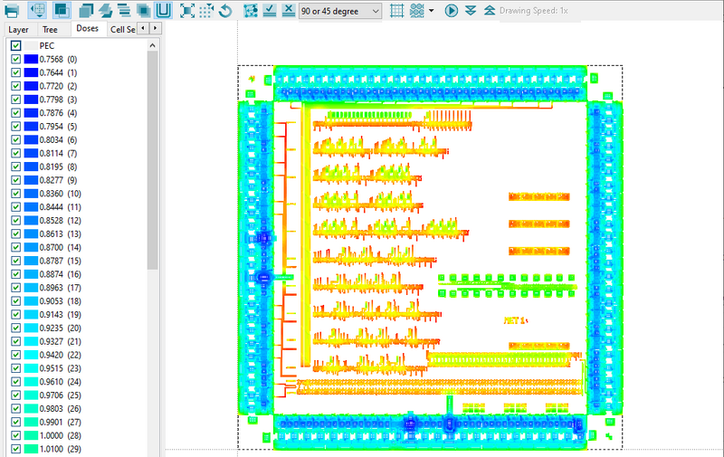
Once a PEC node has been applied to a design and executed the design is broken into a number of shot ranks. Each shot rank has a specific dose associated with it. The doses and and how they are applied to the pattern can be seen in the pattern viewer by clicking on the Color by Dose button and selecting the Dose tree. In general, large and dense strcutures will be modulated down in dose to accuont for abundant backscatter exposure while small and sparse features will be modulated to a higher dose since there is little backscatter exposure in those areas.
|
|
Dose modulation as generated by a PEC process. |
Export to V30
As a final step to pattern preparation it must be exported to the V30 format. This is done by connecting a Export node to the flow. In the first window that opens make sure to choose V30 as the file format.
The Export node itself has quite a few options. The most import is the Machine Type field which defaults to an incorrect machine. Make sure to choose JBX-9500FS (100kV). In most cases all other options can be left at their default values. There can however be good reasons to control the fracturing and field ordering found in the Advanced tab. For information on these please check the respective sections of our Beamer guide.
In addition to the V30 file a .JDI file is also generated. This contains the corresponding dose modulation table. If the design is not proximity corrected the table will be empty and is not needed. If the design is proximity corrected it is necesarry to open the JDI file and copy-paste the modulation table into the JDF file used for the exposure.
| Example JDI file after PEC |
|---|
MOD001: MODULAT (( 0, -24.3 ) , ( 1, -23.6 ) , ( 2, -22.8 ) - , ( 3, -22.0 ) , ( 4, -21.2 ) , ( 5, -20.5 ) - , ( 6, -19.7 ) , ( 7, -18.9 ) , ( 8, -18.0 ) - , ( 9, -17.2 ) , ( 10, -16.4 ) , ( 11, -15.6 ) - , ( 12, -14.7 ) , ( 13, -13.9 ) , ( 14, -13.0 ) - , ( 15, -12.1 ) , ( 16, -11.3 ) , ( 17, -10.4 ) - , ( 18, -9.5 ) , ( 19, -8.6 ) , ( 20, -7.7 ) - , ( 21, -6.7 ) , ( 22, -5.8 ) , ( 23, -4.8 ) - , ( 24, -3.9 ) , ( 25, -2.9 ) , ( 26, -2.0 ) - , ( 27, -1.0 ) , ( 28, 0.0 ) , ( 29, 1.0 ) - , ( 30, 2.0 ) , ( 31, 3.0 ) , ( 32, 4.1 ) - , ( 33, 5.1 ) , ( 34, 6.2 ) , ( 35, 7.2 ) - , ( 36, 8.3 ) , ( 37, 9.4 ) , ( 38, 10.5 ) - , ( 39, 11.6 ) , ( 40, 12.7 ) , ( 41, 13.8 ) - , ( 42, 14.9 ) , ( 43, 16.1 ) , ( 44, 17.3 ) - , ( 45, 18.4 ) , ( 46, 19.6 ) , ( 47, 20.8 ) - , ( 48, 22.0 ) , ( 49, 23.2 ) , ( 50, 24.5 ) - , ( 51, 25.7 ) , ( 52, 27.0 ) , ( 53, 28.2 ) - , ( 54, 29.5 ) , ( 55, 30.8 ) , ( 56, 32.1 ) - , ( 57, 33.5 ) , ( 58, 34.8 ) , ( 59, 36.1 ) - , ( 60, 37.5 ) , ( 61, 38.9 ) , ( 62, 40.3 ) - , ( 63, 41.7 ) , ( 64, 43.1 ) , ( 65, 44.5 ) - , ( 66, 46.0 ) , ( 67, 47.4 ) , ( 68, 48.9 ) - , ( 69, 50.4 )) ; SCAN_STEP = 0.001000 ; MINIMAL_RESOLUTION = 0.000250 ; MACHINE_TYPE = JBX-9500FS (100kV) ; DIGITAL_SCALING_X = 1.000000 ; DIGITAL_SCALING_Y = 1.000000 ; MAXIMUM_BEAMSIZE = 16000 ; SHOT_SHIFT_COUNT = 1 ; OVERLAP_COUNT = 1 ; INCREMENT_SCANNER_DATA_UNIT = 1 ; SUBFIELD_SORTING_DIRECTION = YZIG ; PATTERN_SORTING_DIRECTION = XZIG ; PATTERN_WRITING_UNIT_TYPE = POSSET |
