Specific Process Knowledge/Etch/DRIE-Pegasus/processB: Difference between revisions
No edit summary |
|||
| (24 intermediate revisions by 2 users not shown) | |||
| Line 1: | Line 1: | ||
'''Feedback to this page''': '''[mailto:labadviser@nanolab.dtu.dk?Subject=Feed%20back%20from%20page%20http://labadviser.nanolab.dtu.dk/index.php/Specific_Process_Knowledge/Etch/DRIE-Pegasus/processB click here]''' | |||
<!--Checked for updates on 28/6-2023 - ok/jmli --> | |||
<!--Checked for updates on 2/10-2020 - ok/jmli --> | |||
<!--Checked for updates on 14/5-2018 - ok/jmli --> | |||
<!--Checked for updates on 4/9-2025 - ok/jmli --> | |||
{{contentbydryetch}} | |||
== Process B == | == Process B == | ||
Process B | Process B was run on a 150 mm wafer with 12-13 % etch load. | ||
{| border="2" cellpadding="2" cellspacing="1" style="text-align:center;" | {| border="2" cellpadding="2" cellspacing="1" style="text-align:center;" | ||
| Line 93: | Line 100: | ||
=== Results === | === Results === | ||
A number of wafers are patterned with the [[Specific Process Knowledge/ | A number of wafers are patterned with the [[Specific Process Knowledge/Pattern Design/Travka|Travka mask set]] in 4 microns of AZ photoresist. The wafers are then etched using two different durations of process B in the DRIE-Pegasus. | ||
{| | {| | ||
| STYLE="vertical-align: top"| | |||
{| border = 1 | |||
|+ '''Wafers''' | |||
|- | |- | ||
! Wafer number | ! width="70" |Wafer number | ||
! Mask | ! width="70" |Mask | ||
! Process B duration | ! Process B duration | ||
|- | |- | ||
| | | 2 | ||
| Travka 05 | | Travka 05 | ||
| 17 cycles | | 17 cycles, 3:07 mins | ||
|- | |- | ||
| | | 3 | ||
| Travka 05 | | Travka 05 | ||
| 34 cycles | | 34 cycles, 6:14 mins | ||
|- | |- | ||
| | | 5 | ||
| Travka 10 | | Travka 10 | ||
| 17 cycles | | 17 cycles, 3:07 mins | ||
|- | |- | ||
| | | 6 | ||
| Travka 10 | | Travka 10 | ||
| 34 cycles | | 34 cycles, 6:14 mins | ||
|- | |- | ||
| | | 8 | ||
| Travka 20 | | Travka 20 | ||
| 17 cycles | | 17 cycles, 3:07 mins | ||
|- | |- | ||
| | | 9 | ||
| Travka 20 | | Travka 20 | ||
| 34 cycles | | 34 cycles, 6:14 mins | ||
|} | |||
| STYLE="vertical-align: top"| | |||
{| border = 1 | |||
|+ '''Wafers''' | |||
|- | |||
! width="70" |Wafer number | |||
! width="70" |Mask | |||
! Process B duration | |||
|- | |- | ||
| | | 11 | ||
| Travka 35 | | Travka 35 | ||
| 17 cycles | | 17 cycles, 3:07 mins | ||
|- | |- | ||
| | | 12 | ||
| Travka 35 | | Travka 35 | ||
| 34 cycles | | 34 cycles, 6:14 mins | ||
|- | |- | ||
| | | 14 | ||
| Travka 50 | | Travka 50 | ||
| 17 cycles | | 17 cycles, 3:07 mins | ||
|- | |- | ||
| | | 15 | ||
| Travka 50 | | Travka 50 | ||
| 34 cycles | | 34 cycles, 6:14 mins | ||
|- | |- | ||
| | | 17 | ||
| Travka 65 | | Travka 65 | ||
| 17 cycles | | 17 cycles, 3:07 mins | ||
|- | |- | ||
| | | 18 | ||
| Travka 65 | | Travka 65 | ||
| 34 cycles | | 34 cycles, 6:14 mins | ||
|} | |} | ||
|} | |||
After etching each wafer is cleaved in two places: Both cleavage lines run across the [[Specific Process Knowledge/Pattern Design/Travka/fields/Aline|A-line fields]]. This produces three sites on each wafer where the depth of the trenches can be determined using an SEM. | |||
<gallery caption="The results of process B after 17 and 34 cycles of etching" widths="500" heights="350" perrow="2"> | <gallery caption="The results of process B after 17 and 34 cycles of etching" widths="500" heights="350" perrow="2"> | ||
image:Travkatesting1a.jpg| | image:Travkatesting1a.jpg| | ||
image:Travkatesting1b.jpg| | image:Travkatesting1b.jpg| | ||
</gallery> | </gallery> | ||
Latest revision as of 10:40, 4 September 2025
Feedback to this page: click here Unless otherwise stated, the content of this page was created by the dry etch group at DTU Nanolab
Process B
Process B was run on a 150 mm wafer with 12-13 % etch load.
| Parameter | Specification | Average result |
|---|---|---|
| Etch rate (µm/min) | > 10 | 10.7 |
| Etched depth (µm) | 100 | 107 |
| Scallop size (nm) | < 800 | 685 |
| Profile (degs) | 91 +/- 1 | 90.7 |
| Selectivity to AZ photoresist | > 100 | 183 |
| Undercut (µm) | <1.5 | 0.89 |
| Uniformity (%) | < 3.5 | 2.7 |
| Repeatability (%) | <4 | 0.47 |
| Main etch (D->E) | Etch | Dep |
|---|---|---|
| Gas flow (sccm) | SF6 350 O2 35 | C4F8 200 |
| Cycle time (secs) | 7.0 | 4.0 |
| Pressure (mtorr) | 20 (1.5 s) 100 | 25 |
| Coil power (W) | 2800 | 2000 |
| Platen power (W) | 130 (1.5) 40 | 0 |
| Cycles | 55 (process time 10:05) | |
| Common | Temperature 10 degs, HBC 10 torr, Short funnel, with baffle & 5mm spacers | |
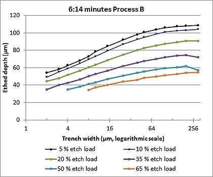
Experiment with process B performance
Purpose
Perhaps the most commonly occuring question posed by users of the dry etch tools is something like ' I want to etch my trenches down to a depth of 40 microns, how long should I etch?'. The answer is that it depends on the width of the trench and on the etch load of your design (that is how many percent of the wafer it etched).
An experiment has been set up to investigate the etched depth of a number of different trenches (with widths ranging from 2 microns to 300 microns) as a function of etch load (the exposed area ranges from 5 % to 65 %)
Results
A number of wafers are patterned with the Travka mask set in 4 microns of AZ photoresist. The wafers are then etched using two different durations of process B in the DRIE-Pegasus.
|
|
After etching each wafer is cleaved in two places: Both cleavage lines run across the A-line fields. This produces three sites on each wafer where the depth of the trenches can be determined using an SEM.
- The results of process B after 17 and 34 cycles of etching
-

-