
Specific Process Knowledge/Thin film deposition/Deposition of CrSi: Difference between revisions
No edit summary |
|||
| (3 intermediate revisions by the same user not shown) | |||
| Line 1: | Line 1: | ||
'''Feedback to this page''': '''[mailto:labadviser@nanolab.dtu.dk?Subject=Feed%20back%20from%20page%20http://labadviser.nanolab.dtu.dk/index.php/Specific_Process_Knowledge/Thin_film_deposition/Deposition_of_CrSi click here]''' | '''Feedback to this page''': '''[mailto:labadviser@nanolab.dtu.dk?Subject=Feed%20back%20from%20page%20http://labadviser.nanolab.dtu.dk/index.php/Specific_Process_Knowledge/Thin_film_deposition/Deposition_of_CrSi click here]''' | ||
<i>This page is written by <b>Evgeniy Shkondin @DTU Nanolab</b> if nothing else is stated. <br> | |||
All images and photos on this page belongs to <b>DTU Nanolab</b>.<br> | |||
The fabrication and characterization described below were conducted in <b>2021-2022 by Evgeniy Shkondin</b> and <b>Henri Jansen, DTU Nanolab</b>.<br></i> | |||
=CrSi as a hard mask= | =CrSi as a hard mask= | ||
| Line 17: | Line 22: | ||
This page presents the results of CrSi bilayer deposition using <b>DC</b> (for Cr) and <b>RF</b> (for Si) Sputtering in Sputter-System Metal-Oxide(PC1) tool commonly known as "Cluster Lesker". The deposition targets are 3" <b>Cr</b> and <b>Si</b>. Source #3(DC) and #1(RF) was used. | This page presents the results of CrSi bilayer deposition using <b>DC</b> (for Cr) and <b>RF</b> (for Si) Sputtering in Sputter-System Metal-Oxide(PC1) tool commonly known as "Cluster Lesker". The deposition targets are 3" <b>Cr</b> and <b>Si</b>. Source #3(DC) and #1(RF) was used. | ||
Spectroscopic Ellipsometry and X-ray reflectivity was used for characterization. The main focus of the study was the deposition rate and thickness measurements. | |||
=Recipe= | =Recipe= | ||
| Line 44: | Line 49: | ||
It must be mentioned that the dark space shield should be in a “closed-form” only, as it was observed that the “opened” dark space shield configuration can do a side wall Cu sputtering. This will heavily contaminate the film and gradually damage the tool. | It must be mentioned that the dark space shield should be in a “closed-form” only, as it was observed that the “opened” dark space shield configuration can do a side wall Cu sputtering. This will heavily contaminate the film and gradually damage the tool. | ||
<gallery caption="Si target with dark space shield configuration and measured uniformity of deposited Si. " widths=" | <gallery caption="Si target with dark space shield configuration and measured uniformity of deposited Si. " widths="400px" heights="350px" perrow="2"> | ||
image:eves_closed_dark_space_shield.png| Closed dark space shield configuration. | image:eves_closed_dark_space_shield.png| Closed dark space shield configuration. | ||
image:eves_Si_120W_20211110.png|Uniformity of deposited Si layer across 6" wafer. | image:eves_Si_120W_20211110.png|Uniformity of deposited Si layer across 6" wafer. | ||
Latest revision as of 13:17, 28 July 2025
Feedback to this page: click here
This page is written by Evgeniy Shkondin @DTU Nanolab if nothing else is stated.
All images and photos on this page belongs to DTU Nanolab.
The fabrication and characterization described below were conducted in 2021-2022 by Evgeniy Shkondin and Henri Jansen, DTU Nanolab.
CrSi as a hard mask
Cr is of particular interest in the dry etch as it serves as a durable hard mask in the quest to go beyond an aspect ratio of 100 in Si etching. To have a Cr pattern the user needs a longer approach. First, the CrSi layer has to be deposited, and then the user has to pattern photoresist. Depending on a feature size a DUV, e-beam, or UV –lithography can be implemented. The photoresist is used to etch the Si layer where the etching stops at the SiCr interface. Finally, a Cr layer is patterned using –F and –O radicals:
The full procedure is described in this article: J. Vac. Sci. Technol. B 39, 032201 (2021) https://doi.org/10.1116/6.0000922
- The sequence of using CrSi as a hard mask
-
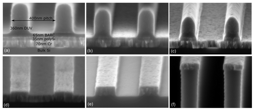 Etch procedure of a 400 nm pitch grating pattern composed of 360 nm thick DUV resist on top of the sample stack: bulk Si + 70 nm Cr + 30 nm polySi + 65 nm Barc. The sample is etched without braking vacuum in the same system in a single run: (a) the initial measures before the etch, (b) after O-based directional Barc etch, (c) directional polySi etch, (d) isotropic polymer strip, (e) directional Cr etch, and (f) the final transfer into the bulk Si. Source: J. Vac. Sci. Technol. B 39, 032201 (2021)

CrSi Sputtering in Sputter-System Metal-Oxide(PC1)
This page presents the results of CrSi bilayer deposition using DC (for Cr) and RF (for Si) Sputtering in Sputter-System Metal-Oxide(PC1) tool commonly known as "Cluster Lesker". The deposition targets are 3" Cr and Si. Source #3(DC) and #1(RF) was used.
Spectroscopic Ellipsometry and X-ray reflectivity was used for characterization. The main focus of the study was the deposition rate and thickness measurements.
Recipe
The process in a Sputter-System Metal-Oxide(PC1) is based on two recipes:
- Single run recipe:
PEG2_PC1_Src3_and_Src1_upstream_CrSi
- Batch recipe:
MDC_PC1_Src3Src1-CrSi_UpsreamPEG2
- Deposition mode: Upstream
- Rotation speed: 10 rpm
- Pressure: 3 mTorr
- Power for Cr: 350 W
- Power for Si: 120 W (It is recomended to use 120W for best uniformity and optical constants fitting).
- Deposition rate: 0.33 nm/s for Cr and 0.029 nm/s for Si.
- Deposition temperature: room temperature
As it is mentioned above the DC source is used for Cr and the RF source is for Si.
The depositions of Si (RF) performed with closed dark space shield configuaration (see photography below).
It must be mentioned that the dark space shield should be in a “closed-form” only, as it was observed that the “opened” dark space shield configuration can do a side wall Cu sputtering. This will heavily contaminate the film and gradually damage the tool.
- Si target with dark space shield configuration and measured uniformity of deposited Si.
-
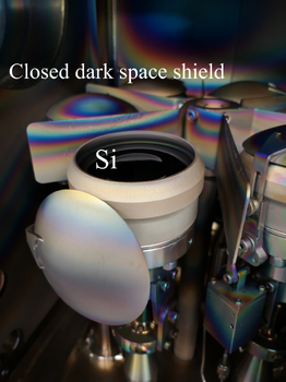 Closed dark space shield configuration.
 -
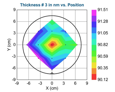 Uniformity of deposited Si layer across 6" wafer.


Sample for Si deposition investigation was 6" Si wafer with 300nm SiO2 (from furnace C1 recipe: DRY1100 05:00:00 + 20 min annealing). However, there is a dedicated page for Si sputtering only.
X-ray Reflectivity Analysis
X-ray reflectivity (XRR) profiles for CrSi films at two different thicknesses (10/10 nm and 30/30 nm) has been obtained using Rigaku XRD SmartLab equipment. The voltage and current settings for the Cu X-ray tube were standard 40kV and 30mA. The incident optics contained a IPS (incident parallel slit) adaptor with 5 ° Soller slit. Other slits: IS=0.03mm RS1=0.03mm and RS2=0.075mm. Step size: 0.01 and measurement time - 5s for each point. Fitting procesure was performed using commercial GlobalFit software assuming the model based on Si substrate with native oxide followed by the deposited CrSi film with thin oxides and moisture surfaces. The results are summarized in a tables below.
- Sample model used in XRR analysis.
-
 Sample considers to have CrSi layer with oxide interlayers and top moisture deposited on natively oxidized silicon.

10nm/10nm
| Layer parameter list | |||||
|---|---|---|---|---|---|
| Layer name | Thickness (nm) | Density (g/cm3) | Rougness (nm) | Delta | Beta |
| Moisture | 0.20 | 0.82 | 0.41 | 2.5278e-6 | 5.8699e-8 |
| SiO2 (native oxide) | 0.53 |
1.59 | 0.22 | 4.7577e-6 | 6.2002e-8 |
| a-Si (sputtered) | 15.46 |
2.31 | 0.00 | 7.5294e-6 | 1.7484e-7 |
| Cr2O3 (interlayer) | 0.30 |
6.61 | 0.60 | 2.0025e-5 | 1.3935e-6 |
| Cr (sputtered) | 11.95 |
7.18 | 0.00 | 2.1109e-5 | 2.1710e-6 |
| SiO2 (native oxide) | 0.78 | 2.03 | 0.42 | 6.4831e-6 | 8.4487e-8 |
| Si (wafer) | 2.328 | 0.00 | 7.5795e-6 | 1.7601e-7 | |
- XRR analysis of 10/10nm CrSi bilayer.
-
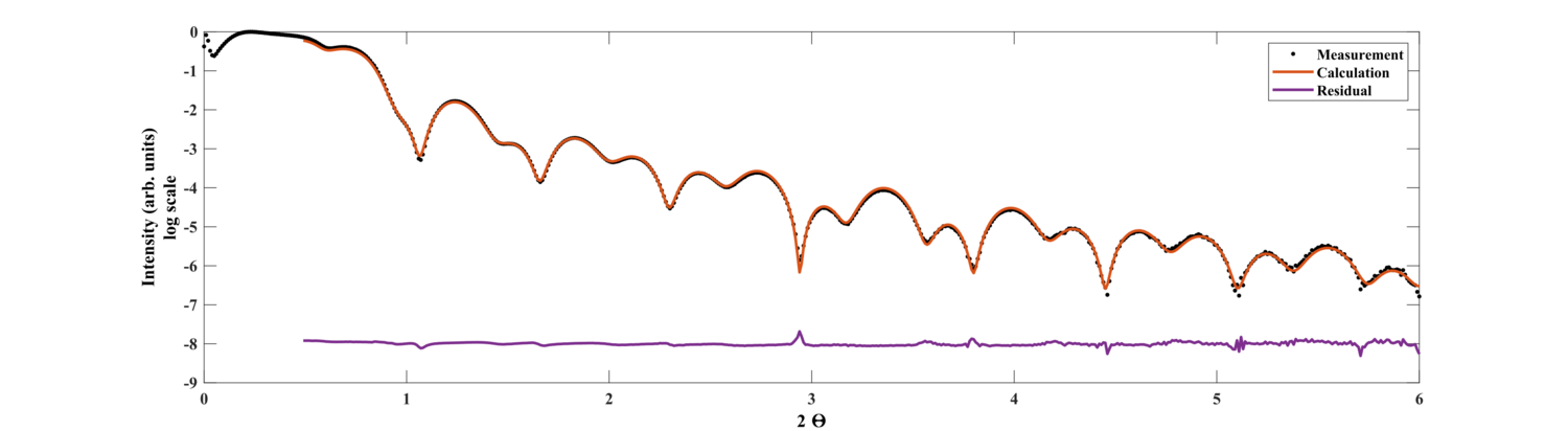 X-ray reflectivity. Measurement and Fit.

30nm/30nm
| Layer parameter list | |||||
|---|---|---|---|---|---|
| Layer name | Thickness (nm) | Density (g/cm3) | Rougness (nm) | Delta | Beta |
| Moisture | 0.70 | 0.64 | 0.1.39 | 1.8383e-6 | 4.2687e-8 |
| SiO2 (native oxide) | 2.28 |
2.32 | 0.87 | 7.5375e-6 | 9.8229e-8 |
| a-Si (sputtered) | 30.94 |
2.34 | 0.00 | 7.6152e-6 | 1.7684e-7 |
| Cr2O3 (interlayer) | 0.45 |
6.72 | 1.13 | 2.0379e-5 | 1.4181e-6 |
| Cr (sputtered) | 26.19 |
7.09 | 0.00 | 2.0846e-5 | 2.1440e-6 |
| SiO2 (native oxide) | 1.54 | 2.48 | 0.42 | 8.0544e-6 | 1.0497e-7 |
| Si (wafer) | 2.328 | 0.04 | 7.5795e-6 | 1.7601e-7 | |
- XRR analysis of 30/30nm CrSi bilayer.
-
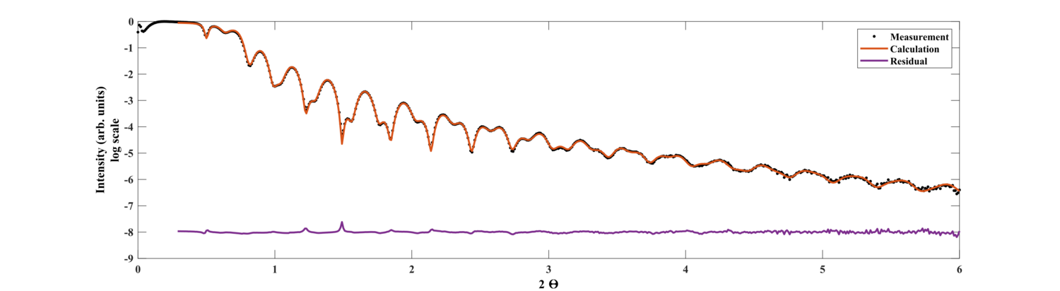 X-ray reflectivity. Measurement and Fit.
