Specific Process Knowledge/Etch/DRIE-Pegasus/Pegasus-4/Slow etch: Difference between revisions
No edit summary |
No edit summary |
||
| (3 intermediate revisions by the same user not shown) | |||
| Line 58: | Line 58: | ||
|- | |- | ||
|Etch rate of SiO2 | |Etch rate of SiO2 | ||
|'''~42nm/min [41-43 nm/min over a 6" wafer] | |'''~42nm/min [41-43 nm/min over a 6" wafer] | ||
|'''13.7-14.7 nm/min [4" on carrier] | |'''13.7-14.7 nm/min [4" on carrier] | ||
| Line 82: | Line 82: | ||
==Etch Profile SEM images== | ==Etch Profile SEM images== | ||
<gallery caption="Profile of etch for 'Slow Etch2' 12 min, 100mm wafer on 150mm carrier with double side polyimide tape (capton)" widths="300px done by bghe, DTU Nanolab" heights="300px" widths="400px" perrow="3"> | <gallery caption="Profile of etch for 'Slow Etch2' 12 min, 100mm wafer on 150mm carrier with double side polyimide tape (capton), Si3N4 from LPCVD" widths="300px done by bghe, DTU Nanolab" heights="300px" widths="400px" perrow="3"> | ||
File:C08507_01.jpg | File:C08507_01.jpg | ||
File:C08507_02.jpg | File:C08507_02.jpg | ||
| Line 102: | Line 102: | ||
File:Contour Plot etch rates Si.jpg|Etch rate map of Si etch on 4" wafer (on 6" carrier) | File:Contour Plot etch rates Si.jpg|Etch rate map of Si etch on 4" wafer (on 6" carrier) | ||
</gallery> | </gallery> | ||
==Test section - do not use== | |||
{| class="wikitable" | |||
|+ Caption text | |||
|- | |||
! A !! Header text !! Header text | |||
|- | |||
| Example || Example || Example | |||
|- | |||
| Example || Example || Example | |||
|- | |||
| Example || Example || Example | |||
|} | |||
Latest revision as of 13:38, 14 July 2025
The slow etch
This work is done by Berit Herstrøm @DTU Nanolab, is nothing else is stated
The slow etch is designed to etch slow at low powers to etch thin films and to avoid overheating of samples mounted on a carrier with Capton/polyimide tape
| Parameter | Recipe name: Slow Etch | Recipe name: Slow Etch2 |
|---|---|---|
| Coil Power [W] | 350 | 200 |
| Platen Power [W] | 25 | 50 |
| Platen temperature [oC] | 20 | 20 |
| H2 flow [sccm] | 15 | 15 |
| CF4 flow [sccm] | 30 | 30 |
| Pressure [mTorr] | 3 | 10 |
| Typical results | Slow Etch | Slow Etch2 |
|---|---|---|
| Etch of SRN | ~43nm/min [measured 39-50 nm/min over a 6" wafer] | 23-25 nm/min [4" on carrier]] |
| Etch rate of Si3N4 | ~49 nm/min [4" on carrier] | 24-26 nm/min [4" on carrier] |
| Etch rate of SiO2 | ~42nm/min [41-43 nm/min over a 6" wafer] | 13.7-14.7 nm/min [4" on carrier] |
| Etch rate in Si | ñm/min | 11-13 nm/min (10% load, 4" wafer on 6" carrier) |
| Etch rate of Mir resist | ~nm/min | ~17 nm/min |
| Tested etch time without burning the resist | 3 min (6 min => resist burned) | 30 min |
| Profile [o] |
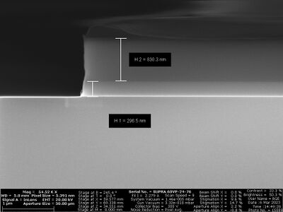
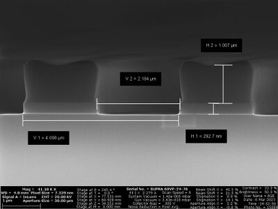
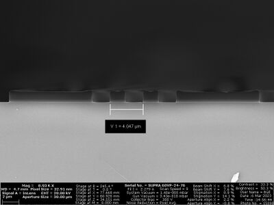
Etch Profile SEM images
- Profile of etch for 'Slow Etch2' 12 min, 100mm wafer on 150mm carrier with double side polyimide tape (capton), Si3N4 from LPCVD
-
-
-


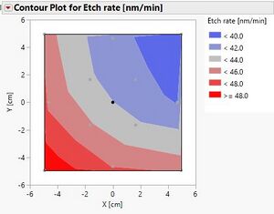
Etch Uniformity maps
- Map of etch rate measurements for 'Slow Etch'
-
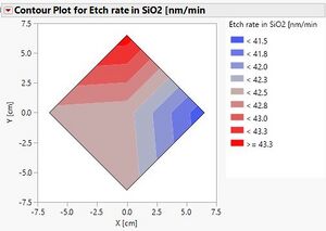 Etch rate map of SiO2 etch on 6" wafer
 -
 Etch rate map of SRN etch on 6" wafer


- Map of etch rate measurements for 'Slow Etch2'
-
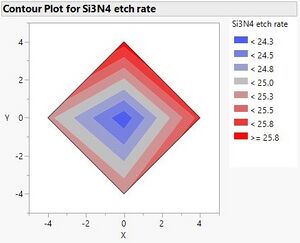 Etch rate map of Si3N4 etch on 4" wafer (on 6" carrier)
 -
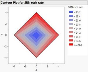 Etch rate map of SRN etch on 4" wafer (on 6" carrier)
 -
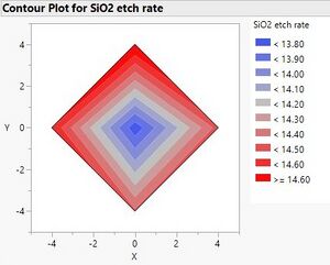 Etch rate map of SiO2 etch on 4" wafer (on 6" carrier)
 -
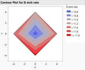 Etch rate map of Si etch on 4" wafer (on 6" carrier)


Test section - do not use
| A | Header text | Header text |
|---|---|---|
| Example | Example | Example |
| Example | Example | Example |
| Example | Example | Example |