
Specific Process Knowledge/Process Flow: Difference between revisions
mNo edit summary |
|||
| (2 intermediate revisions by the same user not shown) | |||
| Line 1: | Line 1: | ||
[[Category:346]] | |||
=The Process Flow= | =The Process Flow= | ||
A Process Flow contains the sequence of steps and techniques used to create certain structures and devices at the microscopic and nanoscopic scales. This involves a combination of various fabrication methods and inspection techniques to achieve the desired features and functionalities. | A Process Flow contains the sequence of steps and techniques used to create certain structures and devices at the microscopic and nanoscopic scales. This involves a combination of various fabrication methods and inspection techniques to achieve the desired features and functionalities. | ||
| Line 92: | Line 88: | ||
| width="150" align="center" style="color:black"| Characterize your Sample[[image:JehanCharacterize.png|130px|frameless|link=Specific Process Knowledge/Characterization]] | | width="150" align="center" style="color:black"| Characterize your Sample[[image:JehanCharacterize.png|130px|frameless|link=Specific Process Knowledge/Characterization]] | ||
| width="150" align="center" style="color:black"| Cut & Pack your Sample (Backend) <br> <br> [[image:JehanPack.png|130px|frameless|link=Specific Process Knowledge/Back-end processing|Back-end processing, also called Assembly and Packaging, are typical processes used to finish up the wafer/chip fabrication, f.ex. wafer thinning, dicing into chips, bonding to a carrier and connecting it with wires to a printed circuit board (PCB).]] | | width="150" align="center" style="color:black"| Cut & Pack your Sample (Backend) <br> <br> [[image:JehanPack.png|130px|frameless|link=Specific Process Knowledge/Back-end processing|Back-end processing, also called Assembly and Packaging, are typical processes used to finish up the wafer/chip fabrication, f.ex. wafer thinning, dicing into chips, bonding to a carrier and connecting it with wires to a printed circuit board (PCB).]] | ||
| width="150" align="center" style="color:black"| Process Flow Examples [[image:Processflow b.png|130px|frameless|link= | | width="150" align="center" style="color:black"| Process Flow Examples [[image:Processflow b.png|130px|frameless|link=LabAdviser/Process Flow/Solar cell process flow|We have made the process flow for a simple solar cell available. It shows you how to build up a process flow for a component that can be made at DTU Nanolab.]] | ||
|- | |- | ||
|} | |} | ||
Latest revision as of 23:05, 1 July 2025
The Process Flow
A Process Flow contains the sequence of steps and techniques used to create certain structures and devices at the microscopic and nanoscopic scales. This involves a combination of various fabrication methods and inspection techniques to achieve the desired features and functionalities.
Starting a process flow from scratch with little or no previous knowledge can be challenging. Please do not hesitate to reach out to colleagues, other cleanroom users or our Fabrication Support team at nanolabsupport@nanolab.dtu.dk for help with your process, discussions regarding problems or improvement.
Below are some recommendations on how to set up a process flow and more information on the different parts of a process flow, including an overview of various process steps. You can then find more detailed information about equipment, processes and materials available on the specific subpages. We also recommended to have a look at the process log on www.labmanager.dtu.dk for the specific machine to check which process parameters or programs other users (f.ex. group members) are using.
You might also have special requirements in your process flow. Please find below a short description of how to get approval for new chemicals or processes.
If you are a new user to DTU Nanolab and you have issues on how to get started in our cleanroom, please have a look at following pages in labadviser: "Safety" and "Getting Started".
General Overview of a Process Flow
- Credentials (title, author, affiliation name, version/batch number, page numbers)
- Pattern design and mask (name and layers)
- Processes & Equipment
- Inspection & Analysis Equipment
- Substrates
- Chemicals
- Special Materials
- Illustrations of Key Process Steps
Review of your Process Flow
Before implementing new processes, we strongly recommended you to get your process validated by our Fabrication Support team. This is done to ensure safety to all cleanroom users and to guard involved machinery and equipment during the processing, e.g. avoid cross-contamination issues, as well as to support your work in the cleanroom. Process flows or any questions regarding process flow review can be submitted to nanolabsupport@nanolab.dtu.dk.
Process Flow Template
You can download a process flow template below and fill it in with your own information. Of course, you are also welcome to make your own template. You are also welcome to take a look at our example for the fabrication of a simple solar cell. It shows you how to build up a process flow for a component that can be made at DTU Nanolab. Throughout the example, you can find links to relevant pages in LabAdviser where information about the different processes are given. Please note that there is also a possibility to create a process flow in Labmanger using the Flow editor.
Process flow template: Process_flow_template_v3.1.docx
Process flow example: Solar Cell Process flow
In the following sections, you can find some guidelines and relevant information for creating your own process flow, such as relevant information about substrate, pattern design and mask fabrication, as well as process steps and characterization methods.
Substrate
Generally, there is a wide range of substrates available for cleanroom processing. This includes silicon, fused silica, III-V substrates, SOI wafers, but also rarer and more expensive materials such as silicon carbide, saphire, and diamond are possible. In some occasions, even different types of polymer can be processed at DTU Nanolab.
DTU Nanolab has a stock of standard silicon and glass wafers that can be purchased through LabManager (requires login). You can find more information on wafers available and how to purchase them through LabManager under Wafer Information. Other substrates have to be purchased personally, though you are very welcome to ask us for help if needed.
There are various sizes and shapes of substrates available. F.ex. standard silicon wafers are available as 2", 4", and 6" and our tools are mostly set up for these dimensions, though some tools can take chips or even 8" wafers. You can find more information on which sizes are able to be processed on the specific equipment page on labadviser or labmanager.
Bringing samples into the cleanroom
Please be aware that you must obtain permission from our Fabrication Support team to bring substrates from outside into our cleanroom. You need to fill out the form "Request to bring Samples into CR v1.51" and submit it to nanolabsupport@nanolab.dtu.dk. Please find more information under Bring samples into cleanroom.
Pattern Design and Mask Preparation
One of the first steps in a fabrication process often involves designing the pattern of the device and, if required, preparing a mask for f.ex. a photo or electron beam lithography step. There are several commercial and free CAD tools available, f.ex. Clewin, KLayout, or L-Edit.
You can find extensive information on how to create a design on following subpages
- UV Lithography (pattern design and order of physical mask)
- DUV Lithography (Reticle Design)
- Electron Beam Lithography (pattern preparation for Jeol exposure)
Fabrication Steps
There is a large variety of cleanroom methods that can be combined within the same Process Flow. Special attention has to be paid to Cross Contamination and compatibility of layers on your substrate with subsequent fabrication steps. For example, oxidation and LPCVD furnaces are often extremely clean and any contamination can damage the functionality of the thin film. Therefore, wafers processed in other machines, such as dry etching equipment, require special cleaning to avoid cross-contamination. Another example is temperature compatibility. The growth of oxide requires very high temperatures, which not all thin films can tolerate without undergoing a major change in f.ex. layer compostion.
Below you can find an overview over some standard fabrication steps with links to their process specific pages in Labadviser. Below the table, there are some examples to specific processes with a list of information that needs to be defined for each process. You can find more examples for fabrication steps and what to remember further below.
Drawings in this section done by Jesper Hanberg @DTU Nanolab
Clean your Sample 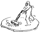
|
Dry your Sample 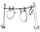
|
Deposit a Thin Film 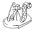
|
Dope your Sample 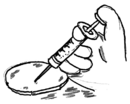
|
Thermal treatment of your Sample 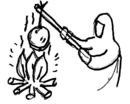
|
Create a Mask on your Sample 
|
Transfer a Pattern to your Sample 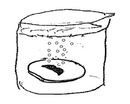
|
Create your Structures in Polymer 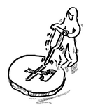
|
Bond your Samples together 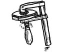
|
Characterize your Sample
|
Cut & Pack your Sample (Backend) 
|
Process Flow Examples 
|
Examples for Information relevant to a Specific Process Step
Please find below some examples that might help you to create a complete process step. If you need assistance, do not hesitate to contact our Fabrication Support Team.
Create a Mask on your Sample (Photolithography Step)
- Specify the design/mask-name, -layers, and polarity used for each photolithography step
- Specify if required and type of alignment (frontside, backside), and if relevant note down alignment marks coordinates
- Specify resist and resist thickness (defines spin process)
- Specify developer
- Specify Spin Coating equipment and process (depending on resist type and thickness)
- Specify Aligner equipment and process including exposure conditions (f.ex. exposure dose)
- Specify Developer equipment and process (depending on resist type and thickness)
- Define tolerance or other inspection criteria
- Check cross-contamination with pre- and post process equipment
Deposit a Thin Film on your Sample (Metal Evaporation)
- Specify metal thicknesses, and deposition rate
- Specify Evaporator equipment, process name
- Define tolerance or other inspection criteria
- Check cross-contamination with pre- and post process equipment
Transfer a Pattern to your Sample (Dry etching)
- Specify Etching Tool
- Specify process name, etch parameters, etch depth
- Define tolerance or other inspection criteria
- Check cross-contamination with pre- and post process equipment
Characterization
A crucial and often neglected part of each process flow is the characterization. After critical process steps you might need to analyze and measure the properties of produced structures, layers, materials or entire devices. Characterization techniques help you ensure that the fabricated components meet the required specifications and function correctly. There are many tools and methods available to inspect, analyze and measure the properties of features and materials such as physical, chemical, electrical, and mechanical properties.
Even if some of these methods are fast and cheap to perform, not all information might be relevant for the fabrication of your device taking up unnecessary resources. It is, therefore, vital to chose methods relevant for you process and product. Please do not hesitate to reach out to our Fabrication Support team at nanolabsupport@nanolab.dtu.dk.
Below we will try to sum up some of the more typical characterization methods, but for now, please have a look at the Characterization page.
THIS PART IS UNDER CONSTRUCTION
Surface Toppography
Analysis of form, shape, size, structure, and surface features including surface roughness, f.ex
- Light microscopy
- Electron beam microscopy: SEM; TEM
- AFM
- Optical or mechanical profilometer
- Particle Scanner
Chemical Composition and Molecular Interaction
Techniques to identify elemental composition and chemical states, as well as the interaction between molecules, f.ex.
- EDS/EDX (Energy Dispersive X-ray Spectroscopy)
- XPS (X-ray Photoelectron Spectroscopy)
- XRD (X-ray diffraction)
- Contact Angle Measurement
- SIMS (Secondary Ion Mass Spectrometry) – not available at DTU Nanolab
- Raman Spectroscopy - not available at DTU Nanolab
Optical Properties
Analysis of optical properties such as film thickness, optical constants (refractive index, extinction coefficient), reflectivity, and others, f.ex.
- Ellipsometry
- Spectrophotometry
- Microspectrophotometer
- PhotoLuminescence Mapper
Mechanical Properties
Techniques to measure hardness, elasticity, and stress, f.ex.
- Stylus profilometer
- Hardness tester
- AFM
Electrical Properties
Techniques to evaluate conductivity, resistivity, and carrier behavior, f.ex.
- 4-Point Probe, Probe station
- III-V ECV-profiler (Electrochemical Capacitance-Voltage carrier density profiler)
- Lifetime scanner MDPmap
- AFM
Others
- Thermal Properties
- Magnetic Properties
Special Requirements
You might have special requirements in your process that require
- chemicals not already approved and/or available in the cleanroom
- processes not available on our machines
- parameters outside allowed parameter range
- processing materials not allowed or available in an equipment
- others special requirements.
In this section we try to elaborate on a few of these topics. Some might have been mentioned in the DTU Nanolab Introductory Course: Cleanroom in B346. If you still have questions, please contact our Fabrication Support Team.
Approval of Special Materials and Processes (Risk Assessment)
If you require chemicals, substrates or would like to run a new process that are not already approved and/or available in the cleanroom, you need to fill out a Risk Assessment (in danish: "Risikovudering (RA)). In the RA, the intended work process with involved chemicals (including concentrations), safetry equipment and involved risk assessment must be described. The RA form is available in english and danish on Kemibrug. Please note that historically the risk assessment can be called "work place assessment" (or in danish arbejdspladsvudering (APV)).
The completed RA form and the safety data sheet (SDS) from the manufacturer or importer must be send to our Safety Coordinator for evaluation and approval of your process.
Non-Standard chemicals need to be purchased by users themselves. If you need assistance, please contact the Fabrication Support Team.
Specialized Processes and Cross Contamination (Equipment)
For each equipment, our specialists have defined a parameter range in which the tool is safe to operate - safe for the tool and operator, and safe for the samples commonly processed. You must contact the responsible equipment group beforehand, if you want to
- run processes with parameters outside the range specified in the manual
- process materials not allowed in the machine
You can find the respective contact details in labmanager on the "Basic Info" page. You are also welcome to contact the Fabrication Support Team for assistance.