Specific Process Knowledge/Cross Contamination: Difference between revisions
| (40 intermediate revisions by 2 users not shown) | |||
| Line 2: | Line 2: | ||
'''Feedback to this page''': '''[mailto:labadviser@nanolab.dtu.dk?Subject=Feed%20back%20from%20page%20http://labadviser.nanolab.dtu.dk/index.php/Specific_Process_Knowledge/Cross_Contamination click here]''' | '''Feedback to this page''': '''[mailto:labadviser@nanolab.dtu.dk?Subject=Feed%20back%20from%20page%20http://labadviser.nanolab.dtu.dk/index.php/Specific_Process_Knowledge/Cross_Contamination click here]''' | ||
<br> | |||
=< | <br> | ||
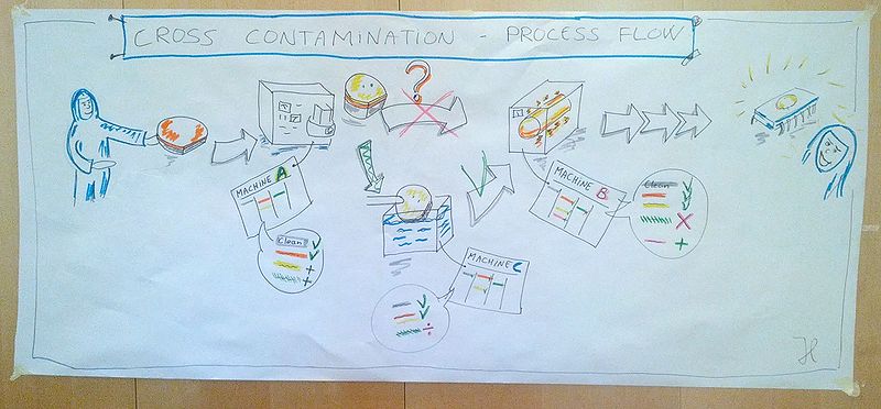
[[image:Cross Contamination - Process Flow.jpg|800px|frameless|link=|The substrate type is characterized by the bulk material characteristics of the given sample.]] | |||
<br> | |||
<br> | |||
= Cross Contamination = | = Cross Contamination = | ||
As explained | As explained on the [[Specific Process Knowledge/Process Flow|'''Process Flow''']] page, there is a large variety of cleanroom fabrication and characterization methods that can be combined to create new materials or structures. Some processes are very sensitive to contaminants and equipment cannot always be cleaned easily running a pre-process cleaning step. | ||
For example, contaminants during a thermal oxidation process to grow silicon dioxide (SiO₂) layers on silicon wafers can significantly degrade the quality and functionality of the resulting oxide layer. Especially metal ions pose a serious issue as they increase leakage currents, reduce the breakdown voltage, reduce the dielectric strength, and cause threshold voltage shifts in MOS devices. But contaminants can also alter the stoichiometry or uniformity of the oxide layer due to non-uniform growth rates and the formation of defective or porous oxides. Therefore, thermal oxidation furnaces have to be maintained extremely clean and the cannot be cleaned easily. | |||
<br> | |||
<br> | |||
{| border="2" style="border: dashed 2px #BB0003" cellspacing="0" cellpadding="10" align="left" | |||
|- | |||
|Please note, as a multiuser facility we need to establish working procedures to provide the best possible working environment for all our users, not only in terms of safety, but also regarding reliability of equipment and processes. '''We expect all users to adhere strictly to the guidelines and equipment usage rules, with particular attention to preventing cross-contamination between tools.''' We are happy to assist you in reviewing and refining your process flow to help streamline your work and ensure compatibility with our facility standards. You can find more information on how to create a process flow [[Specific Process Knowledge/Process Flow|'''here''']]. | |||
|- | |||
|} | |||
<br clear="all"> | |||
<br> | |||
<br> | |||
'''Why care about cross contamination?''' | |||
# Compliance with Cleanroom Standards | # Compliance with Cleanroom Standards | ||
#* Semiconductor fabs operate under strict cleanroom classifications (e.g., ISO 5 or better). | #* Semiconductor fabs operate under strict cleanroom classifications (e.g., ISO 5 or better). | ||
| Line 22: | Line 33: | ||
#* Clean systems are less prone to corrosion, clogging, or mechanical failure. | #* Clean systems are less prone to corrosion, clogging, or mechanical failure. | ||
<br> | <br> | ||
== Cross Contamination Groups in LabManager == | |||
== Cross Contamination | We have created a cross contamination sheet available in Labmanager as a guideline regarding which materials are allowed to enter an equipment. It is also possible to show the cross contamination between two tools. You can find more information below. | ||
We have created a cross contamination sheet available in | |||
Cross contamination can origin from many different sources | Cross contamination can origin from many different sources: the substrate itself, films deposited or grown on top of the substrate, traces from previous processes, and the environment. To make it easier for our users, we have sorted them into groups according to the sources of contamination. | ||
<br> | <br> | ||
<br> | <br> | ||
| Line 64: | Line 74: | ||
<br> | <br> | ||
<br clear="all"> | <br clear="all"> | ||
<br> | |||
Please note, a processed sample can be coated with more than one film. For some processes, only the top layer may be evaluated with respect to cross contamination, f.ex. if buried layers are not exposed during the process and traces can be disregarded for the process. But for other processes, all layers need to be evaluated, f.ex. if you etch through several layers, you will expose underlying material. In that case, all layers need to be considered for the cross contamination. Please contact the equipment responsible group or [mailto:nanolabsupport@nanolab.dtu.dk nanolabsupport@nanolab.dtu.dk], if you have multilayer substrates and you are in doubt if you can process your sample in the respective tool. | |||
<br> | |||
<br> | |||
== How to Access the Cross Contamination Sheet == | |||
Please note that some cross contamination sheets might be outdated. If you are unsure whether you are allowed to process your wafer in a specific equipment, please contact [mailto:training@nanolab.dtu.dk training@nanolab.dtu.dk]. | |||
== How to | <br> | ||
<br> | |||
'''Access Cross Contamination Sheet:''' | |||
* Go to the “Equipment Info” page | * Go to the “Equipment Info” page | ||
* Select the tool | * Select the tool | ||
| Line 83: | Line 97: | ||
<br> | <br> | ||
<br> | <br> | ||
=== Cross Contamination between two Tools === | |||
=== | * Commonly the tool you selected is set as default, else click on "Select other equipment" | ||
* | * Click on "Select "TO" equipment" | ||
* | |||
<br> | <br> | ||
[[image:cross_contamination_between.png|800px|frameless|Example for a cross contamination sheet for the PECVD03]] | [[image:cross_contamination_between.png|800px|frameless|Example for a cross contamination sheet for the PECVD03]] | ||
<br> | <br> | ||
<br> | <br> | ||
To evaluate the viability of your process and cross contamination of your sample, you have to consider | |||
* Is your sample with its particular attributes allowed in the tool? ('''"In"''') | |||
* Does the tool contaminate your sample during processing? ([[image:xcplus.png|15px|frameless|link=]] '''"Out +"''') | |||
* Does the tool remove a particular attribute from your sample during processing? ([[image:xcminus.png|15px|frameless|link=]] '''"Out -"''') | |||
* Are there process dependent attributes or traces added or removed? ([[image:xccaution.png|15px|frameless|link=]]) | |||
<br> | |||
As you can see from the screenshot above, you are not allowed to process a sample in the "Si Etch 1: KOH" bath (our cleanest KOH etch bath) that has been previously been processed in "PECVD03". Your sample might have picked up traces of material list 3, f.ex. silver, gold, or copper during processing in the PECVD03. Since those contaminants can alter the etching process and, even more, contaminate samples processed in "Si Etch 1: KOH", they are forbidden. | |||
= | |||
<br> | |||
Latest revision as of 22:36, 17 June 2025
The content on this page, including all images and pictures, was created by DTU Nanolab staff, unless otherwise stated.
Feedback to this page: click here
Cross Contamination
As explained on the Process Flow page, there is a large variety of cleanroom fabrication and characterization methods that can be combined to create new materials or structures. Some processes are very sensitive to contaminants and equipment cannot always be cleaned easily running a pre-process cleaning step.
For example, contaminants during a thermal oxidation process to grow silicon dioxide (SiO₂) layers on silicon wafers can significantly degrade the quality and functionality of the resulting oxide layer. Especially metal ions pose a serious issue as they increase leakage currents, reduce the breakdown voltage, reduce the dielectric strength, and cause threshold voltage shifts in MOS devices. But contaminants can also alter the stoichiometry or uniformity of the oxide layer due to non-uniform growth rates and the formation of defective or porous oxides. Therefore, thermal oxidation furnaces have to be maintained extremely clean and the cannot be cleaned easily.
| Please note, as a multiuser facility we need to establish working procedures to provide the best possible working environment for all our users, not only in terms of safety, but also regarding reliability of equipment and processes. We expect all users to adhere strictly to the guidelines and equipment usage rules, with particular attention to preventing cross-contamination between tools. We are happy to assist you in reviewing and refining your process flow to help streamline your work and ensure compatibility with our facility standards. You can find more information on how to create a process flow here. |
Why care about cross contamination?
- Compliance with Cleanroom Standards
- Semiconductor fabs operate under strict cleanroom classifications (e.g., ISO 5 or better).
- Equipment cleanliness is essential to meet these standards.
- Maintain Process Integrity
- Clean tools ensure repeatable and predictable results.
- Prevents cross-wafer contamination.
- Protect Sensitive Materials
- Extend Equipment Life
- Clean systems are less prone to corrosion, clogging, or mechanical failure.
Cross Contamination Groups in LabManager
We have created a cross contamination sheet available in Labmanager as a guideline regarding which materials are allowed to enter an equipment. It is also possible to show the cross contamination between two tools. You can find more information below.
Cross contamination can origin from many different sources: the substrate itself, films deposited or grown on top of the substrate, traces from previous processes, and the environment. To make it easier for our users, we have sorted them into groups according to the sources of contamination.
Substrate 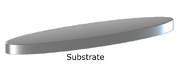
|
Film 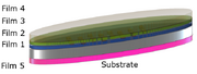
|
Traces 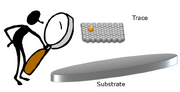
|
Miscellaneous 
|
Examples:
|
Examples:
|
Examples:
|
Examples:
|
Please note, a processed sample can be coated with more than one film. For some processes, only the top layer may be evaluated with respect to cross contamination, f.ex. if buried layers are not exposed during the process and traces can be disregarded for the process. But for other processes, all layers need to be evaluated, f.ex. if you etch through several layers, you will expose underlying material. In that case, all layers need to be considered for the cross contamination. Please contact the equipment responsible group or nanolabsupport@nanolab.dtu.dk, if you have multilayer substrates and you are in doubt if you can process your sample in the respective tool.
How to Access the Cross Contamination Sheet
Please note that some cross contamination sheets might be outdated. If you are unsure whether you are allowed to process your wafer in a specific equipment, please contact training@nanolab.dtu.dk.
Access Cross Contamination Sheet:
- Go to the “Equipment Info” page
- Select the tool
- Click on the button “Cross Contamination Sheet”

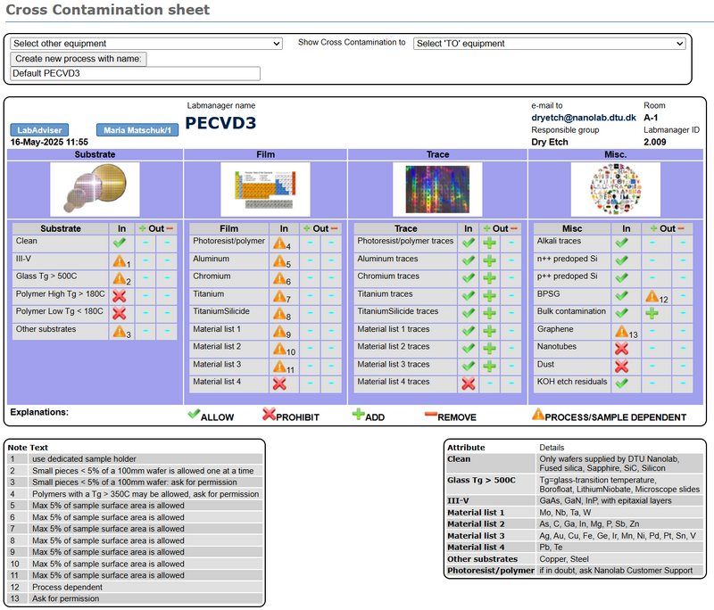
As you can see, there is a long list of substrates that can go into the "PECVD03", even with exposed metal films (area exposed < 5%), as long as they do not contain materials from "material list 4", nanotubes, or dust. Polymers are also not allowed in the equipment.
Cross Contamination between two Tools
- Commonly the tool you selected is set as default, else click on "Select other equipment"
- Click on "Select "TO" equipment"

To evaluate the viability of your process and cross contamination of your sample, you have to consider
- Is your sample with its particular attributes allowed in the tool? ("In")
- Does the tool contaminate your sample during processing? (
 "Out +")
 - Does the tool remove a particular attribute from your sample during processing? (
 "Out -")
 - Are there process dependent attributes or traces added or removed? (
 )
)
As you can see from the screenshot above, you are not allowed to process a sample in the "Si Etch 1: KOH" bath (our cleanest KOH etch bath) that has been previously been processed in "PECVD03". Your sample might have picked up traces of material list 3, f.ex. silver, gold, or copper during processing in the PECVD03. Since those contaminants can alter the etching process and, even more, contaminate samples processed in "Si Etch 1: KOH", they are forbidden.