Specific Process Knowledge/Characterization/X-Ray Diffractometer: Difference between revisions
No edit summary |
mNo edit summary |
||
| (One intermediate revision by the same user not shown) | |||
| Line 1: | Line 1: | ||
The contents on this page, including all images and pictures, was created by DTU Nanolab and DTU Electro staff unless otherwise stated. | |||
'' | '''Feedback to this page''': '''[mailto:nanolabsupport@nanolab.dtu.dk?Subject=Feed%20back%20from%20page%20http://labadviser.nanolab.dtu.dk/index.php?title=Specific_Process_Knowledge/Characterization/X-Ray_Diffractometer click here]''' | ||
<br><br> | |||
'''<p style="color:red;">The X-Ray Diffractometer has been decomissioned. Please find other XRD setups at DTU Nanolab [[Specific Process Knowledge/Characterization/XRD| ''here''.]]</p>''' | |||
= | =Philips DCD IIH X-ray Diffractometer= | ||
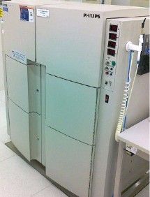
[[file:X-ray_diffractometer.jpg|300px|right|thumb|X-ray diffractometer]] | [[file:X-ray_diffractometer.jpg|300px|right|thumb|X-ray diffractometer]] | ||
The Philips DCD IIH x-ray diffractometer used to characterize the layers on epitaxial semiconductor structures - usually III-V compound semiconductors. | The Philips DCD IIH x-ray diffractometer used to characterize the layers on epitaxial semiconductor structures - usually III-V compound semiconductors. | ||
X-ray diffraction is a non-destructive technique to measure the lattice mismatch of epitaxial grown layers. The resulting measurements are also know as rocking-curves. In this way it is possible to get the relative content of e.g. In in Ga<sub>x</sub>In<sub>1-x</sub>As grown on InP. Ga<sub>0.47</sub>In<sub>0.53</sub>As is lattice-matched to InP. Compunds containing three different materials are also called ternaries. | X-ray diffraction is a non-destructive technique to measure the lattice mismatch of epitaxial grown layers. The resulting measurements are also know as rocking-curves. In this way it is possible to get the relative content of e.g. In in Ga<sub>x</sub>In<sub>1-x</sub>As grown on InP. Ga<sub>0.47</sub>In<sub>0.53</sub>As is lattice-matched to InP. Compunds containing three different materials are also called ternaries. | ||
Latest revision as of 16:20, 2 June 2025
The contents on this page, including all images and pictures, was created by DTU Nanolab and DTU Electro staff unless otherwise stated.
Feedback to this page: click here
The X-Ray Diffractometer has been decomissioned. Please find other XRD setups at DTU Nanolab here.
Philips DCD IIH X-ray Diffractometer

The Philips DCD IIH x-ray diffractometer used to characterize the layers on epitaxial semiconductor structures - usually III-V compound semiconductors.
X-ray diffraction is a non-destructive technique to measure the lattice mismatch of epitaxial grown layers. The resulting measurements are also know as rocking-curves. In this way it is possible to get the relative content of e.g. In in GaxIn1-xAs grown on InP. Ga0.47In0.53As is lattice-matched to InP. Compunds containing three different materials are also called ternaries. For more complex compounds containing 4 elements, known as quaternaries, e.g. GaxIn1-xAsyP1-y, it is possible to obtain both x and y by combining x-ray diffraction measurements and PL-measurements (see PL Mapper).
| Performance | Excitation |
|
|---|---|---|
| Detection |
| |
| Sample size |
| |
| Resolution |
| |
| Materials | Allowed substrate materials |
|
