Specific Process Knowledge/Etch/Aluminum Oxide/Al2O3 Etch using HF: Difference between revisions
m →Photoresist adhesion: formatting |
|||
| (16 intermediate revisions by 4 users not shown) | |||
| Line 1: | Line 1: | ||
''' | '''Unless anything else is stated, everything on this page, text and pictures are made by DTU Nanolab.''' | ||
'''All links to Kemibrug (SDS) and Labmanager Including APV and QC requires login.''' | |||
'''Feedback to this page''': '''[mailto:labadviser@danchip.dtu.dk?Subject=Feed%20back%20from%20page%20http://labadviser.nanolab.dtu.dk/index.php/Specific_Process_Knowledge/Etch/Aluminum_Oxide/Al2O3_Etch_using_HF click here]''' | |||
A wet chemical etch of Al<sub>2</sub>O<sub>3</sub> can be done with HF. The etch rate depends on the HF concentration. | A wet chemical etch of Al<sub>2</sub>O<sub>3</sub> can be done with HF. The etch rate depends on the HF concentration. | ||
| Line 8: | Line 10: | ||
=== Experiment and results === | === Experiment and results === | ||
Si samples with about 100 nm of [[Specific_Process_Knowledge/Thin_film_deposition/ALD_Picosun_R200|ALD]] deposited Al<sub>2</sub>O<sub>3</sub> (1000 cycles at 300<sup>o</sup>C) has been etched in different HF concentrations. After the etching, the thickness of the Al<sub>2</sub>O<sub>3</sub> layer has been measured, and the thickness as function of time has been plotted as shown in the graph below. | Si samples with about 100 nm of [[Specific_Process_Knowledge/Thin_film_deposition/ALD_Picosun_R200|ALD]] deposited Al<sub>2</sub>O<sub>3</sub> (1000 cycles at 300<sup>o</sup>C) has been etched in different HF concentrations. After the etching, the thickness of the Al<sub>2</sub>O<sub>3</sub> layer has been measured using [[Specific_Process_Knowledge/Characterization/Optical_characterization#Ellipsometer|Ellipsometer VASE]], and the thickness as function of time has been plotted as shown in the graph below. | ||
<gallery caption=" | <gallery caption="" widths="600px" heights="500px" perrow="1"> | ||
image:Al2O3_HF_20190826.png| | image:Al2O3_HF_20190826.png| Different etching rates for different HF concentrations. | ||
</gallery> | </gallery> | ||
| Line 17: | Line 19: | ||
The etch rates: | The etch rates: | ||
<ul> | <ul> | ||
<li> 5% HF | <li><p>5% HF → <b>1.74 nm/s</b></p></li> | ||
<li> 1vol. H<sub>2</sub>O : 1vol. 5% HF 1.05 nm/s </li> | <li><p> 1vol. H<sub>2</sub>O : 1vol. 5% HF → <b>1.05 nm/s</b></p></li> | ||
<li> 2vol. H<sub>2</sub>O : 1vol. 5% HF 0. | <li><p> 2vol. H<sub>2</sub>O : 1vol. 5% HF → <b>0.72 nm/s</b></p></li> | ||
</ul> | </ul> | ||
Be aware of that the 5% HF etches quite fast | Be aware of that the 5% HF etches quite fast. Actually, so fast that it can be tricky to control. Taking the sample out of the solution and placing it in a bigger water container to rinse, resulting a time delay due to the movement and the etch continues. It means the handling things around the fumehood can be a source of errors in this case. | ||
''Evgeniy Shkondin, DTU Nanolab, June 2019'' | ''Evgeniy Shkondin, DTU Nanolab, June 2019'' | ||
=== Photoresist adhesion === | |||
Experiments in April 2025 as shown bad adhesion of AZ 5214E on Al2O3. Total delamination occurred in less than 120 seconds on 50nm and 100nm of Al2O3 deposited using ALD. | |||
Thus wetetch is unsuitable to structure an Al2O3 for use as hard-mask for dryetching. | |||
<br> | |||
Systematic studies have not yet been done as of April 2025. | |||
<br> | |||
Following parameters were tested: | |||
{| class="wikitable" | |||
|+ Process parameters | |||
|- | |||
!style="max-width:7em;"| ALD Parameters | |||
|| | |||
* Cycles: 500 and 1000 | |||
* Temperature: 200°C | |||
* TMA pulse: 0.1s | |||
* H2O pulse: 0.1s | |||
|- | |||
!style="max-width:7em;"| Lithography parameters | |||
|| | |||
* Pretreatment: HMDS | |||
* Resist type: AZ 5214E | |||
* Resist thickness: 1.5µm | |||
* Exposure parameters: | |||
** Tool: MLA3 | |||
** Dose: 100 mJ/cm2 | |||
** Defocus: 1 | |||
** Mode: Fast | |||
* Development: TMAH, SP60 | |||
* Post treatment: Hardbake 120s@120C | |||
|} | |||
''Jesper Pan, DTU Nanolab, April 2025'' | |||
Latest revision as of 12:37, 3 April 2025
Unless anything else is stated, everything on this page, text and pictures are made by DTU Nanolab.
All links to Kemibrug (SDS) and Labmanager Including APV and QC requires login.
Feedback to this page: click here
A wet chemical etch of Al2O3 can be done with HF. The etch rate depends on the HF concentration.
Experiment and results
Si samples with about 100 nm of ALD deposited Al2O3 (1000 cycles at 300oC) has been etched in different HF concentrations. After the etching, the thickness of the Al2O3 layer has been measured using Ellipsometer VASE, and the thickness as function of time has been plotted as shown in the graph below.
-
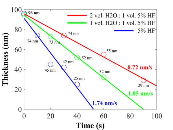 Different etching rates for different HF concentrations.

The etch rates:
5% HF → 1.74 nm/s
1vol. H2O : 1vol. 5% HF → 1.05 nm/s
2vol. H2O : 1vol. 5% HF → 0.72 nm/s
Be aware of that the 5% HF etches quite fast. Actually, so fast that it can be tricky to control. Taking the sample out of the solution and placing it in a bigger water container to rinse, resulting a time delay due to the movement and the etch continues. It means the handling things around the fumehood can be a source of errors in this case.
Evgeniy Shkondin, DTU Nanolab, June 2019
Photoresist adhesion
Experiments in April 2025 as shown bad adhesion of AZ 5214E on Al2O3. Total delamination occurred in less than 120 seconds on 50nm and 100nm of Al2O3 deposited using ALD.
Thus wetetch is unsuitable to structure an Al2O3 for use as hard-mask for dryetching.
Systematic studies have not yet been done as of April 2025.
Following parameters were tested:
| ALD Parameters |
|
|---|---|
| Lithography parameters |
|
Jesper Pan, DTU Nanolab, April 2025