Specific Process Knowledge/Etch/ICP Metal Etcher/Chromium: Difference between revisions
| (3 intermediate revisions by the same user not shown) | |||
| Line 5: | Line 5: | ||
The Chromium etch was carried out on the following substrate stack: | The Chromium etch was carried out on the following substrate stack: | ||
2" Si wafer with Cr laying in a 6" Si wafer with a 4" recess. The area outside the recess was covered by AZ resist. | 2" Si wafer with Cr laying in a 6" Si wafer with a 4" recess. The area outside the recess was covered by AZ resist. | ||
The work was carried out | The work was carried out by Erol Zekovic @Nanotech and BGHE@nanolab | ||
* [[/End point|Cr etch - when to stop using end point detecting]] | |||
{| border="2" cellpadding="2" cellspacing="1" style="text-align:center;" | {| border="2" cellpadding="2" cellspacing="1" style="text-align:center;" | ||
|+ '''Cr etch''' | |+ '''Cr etch''' | ||
| Line 42: | Line 44: | ||
| Was masked by capton tape | | Was masked by capton tape | ||
|} | |} | ||
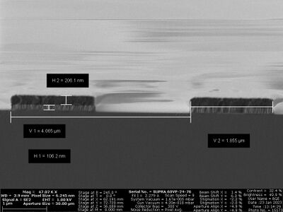
<gallery caption="Etching lines in 100nm Cr with the Cr etch for 3:30 min with 500 nm DUV resist on a 22mmx22mm piece ''BGHE@Nanolab Jan 2023''" perrow="5" widths="400px" heights="300px"> | |||
File:s040321_02.jpg | |||
File:s040321_05.jpg | |||
File:s040321_08.jpg | |||
File:s040321_11.jpg | |||
File:s040321_12.jpg | |||
File:s040321_14.jpg | |||
</gallery> | |||
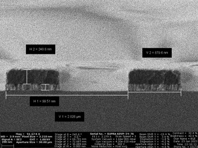
<gallery caption="Etching lines in 100nm Cr with the Cr etch for 3 min with 300 nm DUV resist ''BGHE@Nanolab Feb 2022''" perrow="5" widths="400px" heights="300px"> | <gallery caption="Etching lines in 100nm Cr with the Cr etch for 3 min with 300 nm DUV resist ''BGHE@Nanolab Feb 2022''" perrow="5" widths="400px" heights="300px"> | ||
Latest revision as of 12:39, 18 February 2025
Feedback to this page: click here
The content on this page, including all images and pictures, was created by Berit Herstrøm @ DTU Nanolab (BGHE), unless otherwise stated.
Chromium etch in ICP metal - small substrate using carrier
The Chromium etch was carried out on the following substrate stack: 2" Si wafer with Cr laying in a 6" Si wafer with a 4" recess. The area outside the recess was covered by AZ resist. The work was carried out by Erol Zekovic @Nanotech and BGHE@nanolab
| Parameter | Cr etch |
|---|---|
| Cl2 (sccm) | 65 |
| O2 (sccm) | 15 |
| Pressure (mTorr) | 15 |
| Coil power (W) | 300 |
| Platen power (W) | 15 |
| Temperature (oC) | 50 |
| Spacers (mm) | 100 |
| Etch rate (nm/min) | ~32 (Date: 2014-08-13) |
| Zep520A resist selectivity | NA |
| Comment | Was masked by capton tape |
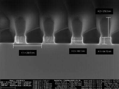
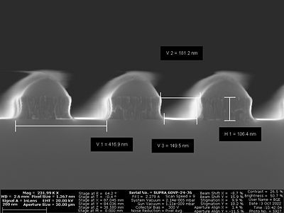
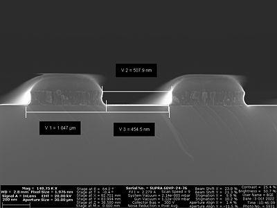
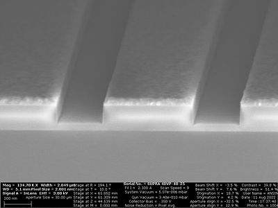
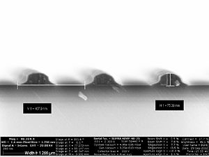
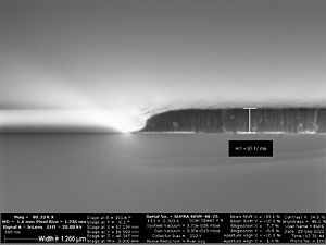
- Etching lines in 100nm Cr with the Cr etch for 3:30 min with 500 nm DUV resist on a 22mmx22mm piece BGHE@Nanolab Jan 2023
-
-
-
-
-
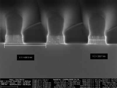
-


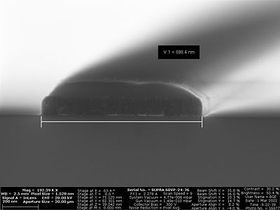
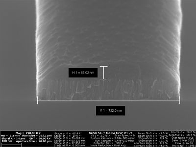
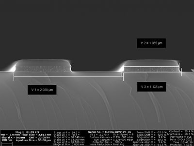
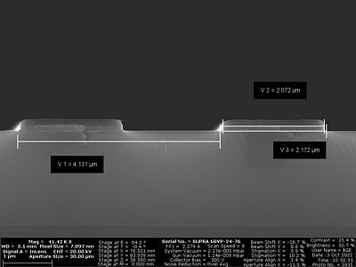
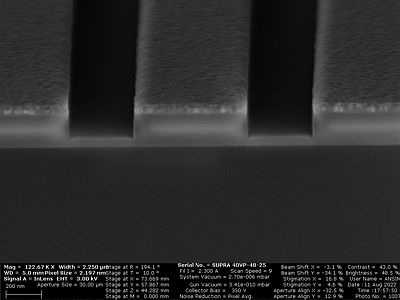
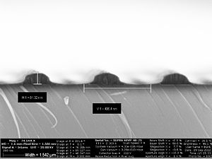
- Etching lines in 100nm Cr with the Cr etch for 3 min with 300 nm DUV resist BGHE@Nanolab Feb 2022
-
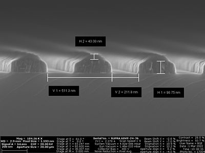
-
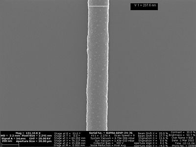
-
-
-
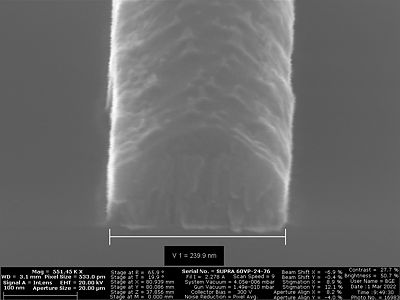


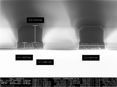
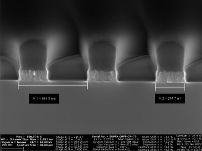
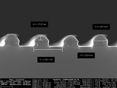
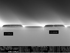
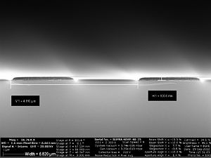
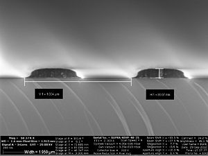
- Etching lines in 100nm Cr with the Cr etch for 3:20 min with pressure of 30 mTorr and 20C with 300 nm DUV resist BGHE@Nanolab Oct 2022
-
-
-
-
-


Chromium etch of hardmask for silicon nitride etching by Anders Simonsen@nbi.ku
This work was done by Anders Simonsen, KU and Added by bghe@Nanolab
Anders has done some work on optimizing the Cr etch for at 30 nm thick Cr that was to be used as masking for a 200nm silicon nitride etch. The Cr etch was carriered out on the ICP metal using 180 nm CSAR and the silicon nitride etch was done on the AOE. You can see his results in this summery that he has made:
- Cr etch development report summery by Anders Simonesen, summer of 2022
- Here are the raw test data and SEM images from Anders Simonsen
Prefered result:
The SEM images where done after both the Cr etch and the silicon nitride etch in the AOE using the recipe "SiN_AS". The important thing was to see how well the Cr works for masking the nitride given vertical and smooth sidewalls in the nitride. The thickness of the Cr was 40 nm
| Recipe | Pressure [mTorr] | Coil power [W] | Platen power [W] | Total Flow Cl2+O2 [sccm] | O2% | Temp | Time [s] | CSAR etch rate [nm/min] | CSAR rate w bond | Etch rate [nm/min] | Selectivity | coil load | coil tune | plat load | plat tune | Comment | |||
|---|---|---|---|---|---|---|---|---|---|---|---|---|---|---|---|---|---|---|---|
| Cr_AS_13 | 10 | 300 | 15 | 30 | 23.33 | 20 | 28 | 100.71 | 42.86 | 0.43 | This recipe was chosen over no. 12 because it did not need a large over etch of the Cr (no foot). |
- After Cr etch with recipe 13 and nitride etch in the AOE 20s
-
 75s Cr etch
 -
 90s Cr etch


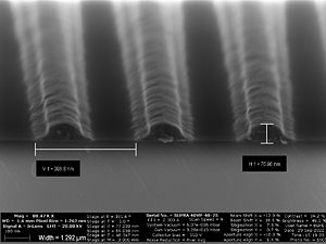
Recipe tried out on DUV pattern with 100 nm Cr and approx. 300 nm DUV resist
by bghe@nanolab 2022-09-29
- A piece of approx 2cmx2cm was bonded to a Si/SiO2 wafer
- 1 min O2 barc etch was done
- 3min20s of CR_AS_13
Results
- Clearly too little resist for this etch
- After Cr etch with recipe Cr_AS_13 for 3min20s
-
-
-
-
-
-
-


Chromium etch in ICP metal on a thick glass substrate
The Chromium etch has ONLY been carried out on the following substrate stack: The Chromium is sputter deposited onto a 2" quartz wafer and patterned by e-beam with Zep520A resist. This 2" QZ wafer is bonded with crystal bond to a 65mmx65mm quartz plate with the thickness: 6.35mm. This QZ plate is bonded to a Si wafer.
| Parameter | Cr etch |
|---|---|
| Cl2 (sccm) | 65 |
| O2 (sccm) | 15 |
| Pressure (mTorr) | 15 |
| Coil power (W) | 300 |
| Platen power (W) | 15 |
| Temperature (oC) | 50 (no back side cooling) |
| Spacers (mm) | 100 |
| Etch rate (nm/min) | ~14 |
| Zep520A resist selectivity | ~0.9 |
| Comment | . |