Specific Process Knowledge/Etch/Etching of Silicon Oxide/SiO2 etch using ASE: Difference between revisions
| (118 intermediate revisions by the same user not shown) | |||
| Line 4: | Line 4: | ||
The ASE is now the "dirty" plasma etcher at Nanolab meaning small amount of metals are allowed to be exposed by the plasma. That calls for recipes etching Silicon oxide and silicon nitride as well as silicon in this machine. | The ASE is now the "dirty" plasma etcher at Nanolab meaning small amount of metals are allowed to be exposed by the plasma. That calls for recipes etching Silicon oxide and silicon nitride as well as silicon in this machine. | ||
= | =CF4/H2 chemistry - SiO2 etch= | ||
''' ''*Unless otherwise stated, all content in this section was done by Maria Farinha@DTU Nanolab, April 2023'' ''' | ''' ''*Unless otherwise stated, all content in this section was done by Maria Farinha@DTU Nanolab, April 2023'' ''' | ||
| Line 30: | Line 30: | ||
|- | |- | ||
|CF<sub>4</sub> flow [sccm] | |CF<sub>4</sub> flow [sccm] | ||
|<center> | |<center>22.5</center> | ||
|<center> | |<center>22.5</center> | ||
|- | |- | ||
|H<sub>2</sub> flow [sccm] | |H<sub>2</sub> flow [sccm] | ||
|<center> | |<center>22.5</center> | ||
|<center> | |<center>22.5</center> | ||
|- | |- | ||
|Pressure [mTorr] | |Pressure [mTorr] | ||
| Line 46: | Line 46: | ||
<br> | <br> | ||
Results of these recipes: | |||
{| border="1" cellspacing="2" cellpadding="2" | {| border="1" cellspacing="2" cellpadding="2" | ||
|-style="background:Black; color:White" | |-style="background:Black; color:White" | ||
! CF4ICP | ! CF4ICP | ||
| | |SiO<sub>2</sub> ER (nm/min) | ||
| | |Selectivity (SiO<sub>2</sub>:resist) | ||
|Si<sub>3</sub>N<sub>4</sub> ER (nm/min) | |||
|Si<sub>x</sub>N ER (nm/min) ^ | |||
|Si ER (nm/min) | |||
|- | |||
|22.5 CF<sub>4</sub> + 22.5 H<sub>2</sub> | |22.5 CF<sub>4</sub> + 22.5 H<sub>2</sub> | ||
|<center> 68 </center> [[File:CF4ICP_11min_C_01.png|200px]] | |||
|<center> 1.13 </center> | |||
|<center> - </center> | |||
|<center> - </center> | |||
|<center> - </center> | |||
|- | |- | ||
|} | |||
^The Si<sub>x</sub>N was deposited in PECVD4, more info in Process log of CF4/H2 tests. | |||
<br> | |||
{| border="1" cellspacing="2" cellpadding="2" | |||
|-style="background:Black; color:White" | |||
! CF4lowCP | |||
|SiO<sub>2</sub> ER (nm/min) | |SiO<sub>2</sub> ER (nm/min) | ||
|< | |Selectivity (SiO<sub>2</sub>:resist) | ||
|< | |Si<sub>3</sub>N<sub>4</sub> ER (nm/min) | ||
|< | |Si<sub>x</sub>N ER (nm/min) | ||
|Si ER (nm/min) | |||
|- | |- | ||
| | |22.5 CF<sub>4</sub> + 22.5 H<sub>2</sub> | ||
|<center> 23.8 </center> [[File:CF4lowCP_20m_pat_C03.png|200px]] | |||
|<center> | |<center> 1.16 </center> | ||
|<center> | |<center> - </center> | ||
|<center> 75.22 (platen 45W) </center> [[File:Si3N4 pat3 cf4lowcp- 1000.png|200px]] | |||
|<center> - </center> | |||
|<center> | |||
|<center> | |||
|<center> | |||
|- | |- | ||
|} | |} | ||
*'''[[/More test with CF4/H2, CHF3 and C4F8/H2 - SiO2 etch|Process log of CF4/H2 tests]]'''</span> | |||
=CHF3/H2 chemistry - SiO2/SiN etch= | |||
''' ''*Unless otherwise stated, all content in this section was done by Maria Farinha@DTU Nanolab, April 2023'' ''' | |||
Due to the instability of older SiO<sub>2</sub> etch recipes, '''''1SIOICP1''''' and '''''TSIO2_02''''', new recipes are being developed, with a CHF<sub>3</sub>/H<sub>2</sub> chemistry. | |||
Two new recipes were created are '''''CHF3_t1''''' and '''''CHF3_t2'''''. The first one aims for thicker etches, with higher ER, while the other is a slower etch, dedicated to thinner layers. | |||
{| border="1" cellspacing="2" cellpadding="2" | {| border="1" cellspacing="2" cellpadding="2" | ||
|-style="background:Black; color:White" | |-style="background:Black; color:White" | ||
! | ! Parameter | ||
| | |Recipe name: '''CHF3_t1''' | ||
| | |Recipe name: '''CHF3_t2''' | ||
| | |- | ||
|Coil Power [W] | |||
|<center>800</center> | |||
|<center>150</center> | |||
|- | |||
|Platen Power [W] | |||
|<center>15</center> | |||
|<center>25</center> | |||
|- | |||
|Platen temperature [<sup>o</sup>C] | |||
|<center>20</center> | |||
|<center>20</center> | |||
|- | |- | ||
| | |CHF<sub>3</sub> flow [sccm] | ||
|<center> | |<center>22.5</center> | ||
|<center>22. | |<center>22.5</center> | ||
|- | |- | ||
| | |H<sub>2</sub> flow [sccm] | ||
|<center> | |<center>22.5</center> | ||
|<center> | |<center>22.5</center> | ||
|- | |- | ||
| | |Pressure [mTorr] | ||
|<center> | |<center>2.5</center> | ||
|<center> | |<center>2.5</center> | ||
|- | |- | ||
|} | |} | ||
CHF<sub>3</sub> and H<sub>2</sub> flow values were changed in order to find the best recipe regarding selectivity SiO<sub>2</sub>/resist and also the uniformity. | |||
<br> | <br> | ||
{| border="1" cellspacing="2" cellpadding="2" | |||
|-style="background:Black; color:White" | |||
! CHF3_t1 | |||
|SiO<sub>2</sub> ER (nm/min) | |||
|Uniformity (SiO<sub>2</sub> etch) | |||
|Selectivity (SiO<sub>2</sub>:resist) | |||
|Si<sub>3</sub>N<sub>4</sub> ER (nm/min) | |||
|Si<sub>x</sub>N ER (nm/min) | |||
|Si ER (nm/min) | |||
|- | |||
|22.5 CHF<sub>3</sub> + 22.5 H<sub>2</sub> | |||
|<center>47.3</center> [[File:CHF3=22.5 H2 10min C 01.png|200px]] | |||
|<center>12%</center> | |||
|<center>1.8</center> | |||
|<center>-</center> | |||
|<center>169.9</center> [[File:Si3N4-pat1-chf3t1-1000.png|200px]] | |||
|<center>-</center> | |||
|- | |||
|} | |||
The uniformity considers a 100mm wafer, calculated with 5 points. | |||
<br> | |||
{| border="1" cellspacing="2" cellpadding="2" | {| border="1" cellspacing="2" cellpadding="2" | ||
|-style="background:Black; color:White" | |-style="background:Black; color:White" | ||
| | ! CHF3_t2 | ||
| | |SiO<sub>2</sub> ER (nm/min) | ||
| | |Uniformity (SiO<sub>2</sub> etch) | ||
| | |Selectivity (SiO<sub>2</sub>:resist) | ||
|Si<sub>3</sub>N<sub>4</sub> ER (nm/min) | |||
| | |Si<sub>x</sub>N ER (nm/min) | ||
| | |Si ER (nm/min) | ||
|- | |- | ||
| | |22.5 CHF<sub>3</sub> + 22.5 H<sub>2</sub> | ||
|[[File: | |<center>27</center> [[File:CHF_t2 nP 10min-05.png|200px]] | ||
| | |<center>-</center> | ||
| | |<center>2^</center> | ||
| | |<center>-</center> | ||
| | |<center>49.9 (platen 45W)</center> [[File:Si3N4-pat2-chf3t2-1000.png|200px]] | ||
| | |<center>-</center> | ||
|- | |- | ||
|} | |} | ||
^This recipe etches resist at high rates depending on the size of the structures. For example, if the structures are smaller, the resist will be eroded away quicker. It's advised to have at least 1:1 ratio of resist to the SiO2 to be etched. | |||
< | *'''[[/tests CHF3+H2 | Results and SEM pictures of CHF3/H2 tests]]'''</span> | ||
= | =C4F8/H2 chemistry - SiO2 etch= | ||
''' ''Unless otherwise stated, all content in this section was done by Maria Farinha@DTU Nanolab, May 2023'' ''' | ''' ''Unless otherwise stated, all content in this section was done by Maria Farinha@DTU Nanolab, May 2023'' ''' | ||
This recipe was taken from the ICP Metal etch, with a slight difference in the platen temperature. This recipe | This recipe was taken from the ICP Metal etch, with a slight difference in the platen temperature. This recipe wasn't yet tested for very deep etches. Be aware of that when processing for more than 10min. You should not process it for more than 20min in a single run, if needed do more runs, you should wait a bit in between processes. | ||
{| border="1" cellspacing="2" cellpadding="2" | {| border="1" cellspacing="2" cellpadding="2" | ||
| Line 173: | Line 222: | ||
!Recipe | !Recipe | ||
!Recipe: SIO2_ICP | !Recipe: SIO2_ICP | ||
!SIO2_ICP on stoic Nit | !SIO2_ICP on stoic Nit (Si<sub>3</sub>N<sub>4</sub>) | ||
!SIO2_ICP on low-stress Nit | !SIO2_ICP on low-stress Nit (Si<sub>x</sub>N) | ||
|- | |- | ||
|Etch rate | |Etch rate | ||
| Line 181: | Line 230: | ||
|194 nm/min | |194 nm/min | ||
(24.05.2023 mfarin @ DTU nanolab) | (24.05.2023 mfarin @ DTU nanolab) | ||
| | | | ||
|- | |- | ||
| Line 237: | Line 285: | ||
<br clear="all" /> | <br clear="all" /> | ||
=SiO2 etch with resist mask, sample on carrier (Si carrier)= | *'''[[/tests C4F8/H2 | tests with C4F8/H2]]'''</span> | ||
=Tests with sample on carrier= | |||
''By Berit Herstrøm @nanolab, January-Marts 2018'' | |||
==SiO2 etch with resist mask, sample on carrier (Si carrier)== | |||
Our old RIE systems have to the end of their lives been used a lot for etching samples that could not be clamped/cooled in the ICP systems. The higher plasma density in the ICP's make their processes more tough on resist masks, probably because of too much heating. Therefor the ICP's are using cooled bottom electrodes with He back side cooling to keep the temperature low for the resist mask to survive. When decommissioning the RIE's (RIE1 and RIE2) a need came for developing recipes on the ICP's that could etch Si, SiO2 and SiN without clamping/cooling the substrates. This part considers etching in SiO2. First an attempt to run the ASE in RIE mode using only the platen generator was made. This resulted in not so nice sidewalls due to redeposition and slow etches, see below. After that the development focused on running with both low coil power and low platen power. | Our old RIE systems have to the end of their lives been used a lot for etching samples that could not be clamped/cooled in the ICP systems. The higher plasma density in the ICP's make their processes more tough on resist masks, probably because of too much heating. Therefor the ICP's are using cooled bottom electrodes with He back side cooling to keep the temperature low for the resist mask to survive. When decommissioning the RIE's (RIE1 and RIE2) a need came for developing recipes on the ICP's that could etch Si, SiO2 and SiN without clamping/cooling the substrates. This part considers etching in SiO2. First an attempt to run the ASE in RIE mode using only the platen generator was made. This resulted in not so nice sidewalls due to redeposition and slow etches, see below. After that the development focused on running with both low coil power and low platen power. | ||
| Line 277: | Line 330: | ||
<br clear="all" /> | <br clear="all" /> | ||
[[/Unstable recipes - SiO2 etch|Unstable SiO2 etch recipes | |||
*<span style="background:#EE4B2B">'''[[/Unstable recipes - SiO2 etch|Unstable SiO2 etch recipes]]'''</span> | |||
Latest revision as of 13:13, 29 April 2024
Feedback to this page: click here
Unless otherwise stated, this page is written by DTU Nanolab internal
The ASE is now the "dirty" plasma etcher at Nanolab meaning small amount of metals are allowed to be exposed by the plasma. That calls for recipes etching Silicon oxide and silicon nitride as well as silicon in this machine.
CF4/H2 chemistry - SiO2 etch
*Unless otherwise stated, all content in this section was done by Maria Farinha@DTU Nanolab, April 2023
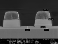
Due to the instability of older SiO2 etch recipes, 1SIOICP1 and TSIO2_02, new recipes are being developed, with a CF4/H2 chemistry. Two new recipes were created, to replace the older ones, CF4ICP and CF4lowCP. The first one aims for thicker etches, with higher ER, while the other is a slower etch, dedicated to thinner layers.
| Parameter | Recipe name: CF4ICP | Recipe name: CF4lowCP |
|---|---|---|
| Coil Power [W] | ||
| Platen Power [W] | ||
| Platen temperature [oC] | ||
| CF4 flow [sccm] | ||
| H2 flow [sccm] | ||
| Pressure [mTorr] |
- CF4 and H2 flow values were changed in order to find the best recipe regarding selectivity between SiO2 and the resist and also the uniformity.
Results of these recipes:
| CF4ICP | SiO2 ER (nm/min) | Selectivity (SiO2:resist) | Si3N4 ER (nm/min) | SixN ER (nm/min) ^ | Si ER (nm/min) |
|---|---|---|---|---|---|
| 22.5 CF4 + 22.5 H2 | 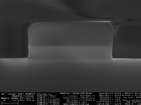
|
^The SixN was deposited in PECVD4, more info in Process log of CF4/H2 tests.
| CF4lowCP | SiO2 ER (nm/min) | Selectivity (SiO2:resist) | Si3N4 ER (nm/min) | SixN ER (nm/min) | Si ER (nm/min) |
|---|---|---|---|---|---|
| 22.5 CF4 + 22.5 H2 | 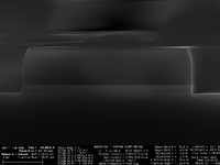
|
|
CHF3/H2 chemistry - SiO2/SiN etch
*Unless otherwise stated, all content in this section was done by Maria Farinha@DTU Nanolab, April 2023
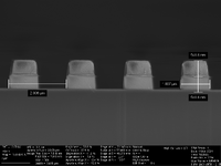
Due to the instability of older SiO2 etch recipes, 1SIOICP1 and TSIO2_02, new recipes are being developed, with a CHF3/H2 chemistry. Two new recipes were created are CHF3_t1 and CHF3_t2. The first one aims for thicker etches, with higher ER, while the other is a slower etch, dedicated to thinner layers.
| Parameter | Recipe name: CHF3_t1 | Recipe name: CHF3_t2 |
|---|---|---|
| Coil Power [W] | ||
| Platen Power [W] | ||
| Platen temperature [oC] | ||
| CHF3 flow [sccm] | ||
| H2 flow [sccm] | ||
| Pressure [mTorr] |
CHF3 and H2 flow values were changed in order to find the best recipe regarding selectivity SiO2/resist and also the uniformity.
| CHF3_t1 | SiO2 ER (nm/min) | Uniformity (SiO2 etch) | Selectivity (SiO2:resist) | Si3N4 ER (nm/min) | SixN ER (nm/min) | Si ER (nm/min) |
|---|---|---|---|---|---|---|
| 22.5 CHF3 + 22.5 H2 | 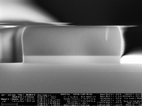
|
|
The uniformity considers a 100mm wafer, calculated with 5 points.
| CHF3_t2 | SiO2 ER (nm/min) | Uniformity (SiO2 etch) | Selectivity (SiO2:resist) | Si3N4 ER (nm/min) | SixN ER (nm/min) | Si ER (nm/min) |
|---|---|---|---|---|---|---|
| 22.5 CHF3 + 22.5 H2 | 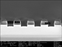
|
|
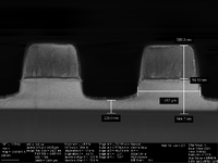
^This recipe etches resist at high rates depending on the size of the structures. For example, if the structures are smaller, the resist will be eroded away quicker. It's advised to have at least 1:1 ratio of resist to the SiO2 to be etched.
C4F8/H2 chemistry - SiO2 etch
Unless otherwise stated, all content in this section was done by Maria Farinha@DTU Nanolab, May 2023
This recipe was taken from the ICP Metal etch, with a slight difference in the platen temperature. This recipe wasn't yet tested for very deep etches. Be aware of that when processing for more than 10min. You should not process it for more than 20min in a single run, if needed do more runs, you should wait a bit in between processes.
| Parameter | Recipe name: SiO2_ICP |
|---|---|
| Coil Power [W] | 1000 |
| Platen Power [W] | 200 |
| Platen temperature [oC] | 20 |
| C4F8 flow [sccm] | 10 |
| H2 flow [sccm] | 28 |
| Pressure [mTorr] | 2.5 |
Results with a non-patterned wafer
| Recipe | Recipe: SIO2_ICP | SIO2_ICP on stoic Nit (Si3N4) | SIO2_ICP on low-stress Nit (SixN) |
|---|---|---|---|
| Etch rate | 121 nm/min
(18.07.2023 mfarin @ DTU nanolab) |
194 nm/min
(24.05.2023 mfarin @ DTU nanolab) |
Results with a patterned wafer
- More tests will be done regarding silicon and silicon nitride, since this recipe can be used for overetch.
Tests with sample on carrier
By Berit Herstrøm @nanolab, January-Marts 2018
SiO2 etch with resist mask, sample on carrier (Si carrier)
Our old RIE systems have to the end of their lives been used a lot for etching samples that could not be clamped/cooled in the ICP systems. The higher plasma density in the ICP's make their processes more tough on resist masks, probably because of too much heating. Therefor the ICP's are using cooled bottom electrodes with He back side cooling to keep the temperature low for the resist mask to survive. When decommissioning the RIE's (RIE1 and RIE2) a need came for developing recipes on the ICP's that could etch Si, SiO2 and SiN without clamping/cooling the substrates. This part considers etching in SiO2. First an attempt to run the ASE in RIE mode using only the platen generator was made. This resulted in not so nice sidewalls due to redeposition and slow etches, see below. After that the development focused on running with both low coil power and low platen power.
SiO2 etch with resist mask, sample on carrier (Si carrier) in the RIE mode using CF4/CHF3/H2 chemistry
By Berit Herstrøm @nanolab, January-Marts 2018
In this study a design of experiments (DOE) were done in RIE mode, meaning using only the platen power and avoiding the coil power. This was to keep the temperature of the substrate low without helium backside cooling the sample.
Results for the DOE
- Redeposition Media:REdeposition ASE_SiO2_RIE_01_design + results - Fit Least Squares.pdf
- Etch rate Media:Etch rate ASE_SiO2_RIE_01_design + results - Fit Least Squares.pdf
- Some Images of the DOE experiments
- PDF file: SEM images of the outcome of the DOE: comparing the level of re-deposition and profiles Media:Compare redeposition.pdf
Conclusion
The conclusion of this work was that using that platen power alone was giving too much re-deposition on the sidewalls leading to very rough sidewalls. To reduce/avoid it the platen power had to be lowered so much that the etch rate got unacceptably low. There for next study included the coil power.
SiO2 etch with resist mask, sample on carrier (Si and Al carrier) in the ICP mode using C4F8/H2/He chemistry
By Berit Herstrøm @danchip, January-Marts 2018
The challenge was to develop a SiO2 etching recipe that can be used for samples on a carrier. Samples that cannot be clamped and cooled. The goal was to keep a good selectivity to the resist mask and get a vertical sidewall, without getting a lot of redeposition on the sidewalls. The testing regime was using both the coil power and the platen power with C4F8/H2 chemistry. Please be aware that some of these recipes are no longer allowed to be run due to too high power without cooling may damage the electrode!
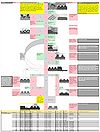 Take a look at development flow and the results here: Media:ASE SiO2 etch on carrier ICP C4F8 H2 no He rev02.pdf . Zoom in to read and see the images: (Ctrl + "+")
Effect chart made from the observations in this study
| Effect chart of increasing input factors | Etch rate | Selectivity to resist | Sidewall | Other Observations |
|---|---|---|---|---|
| Coil power ↑ | ↑ | ↓ | At high coil powers the sample surface gets so hot that it affects the resists too much. The resist changes form at the high powers and the plasma/ions breaks through the resist at different rates, leaving the SiO2 surface very rough. 150W seems to be good for etching about 1 µm of SiO2. Remember this is for samples that are NOT clamped and cooled. | |
| Platen power ↑ | ↑ | ↓ | High Platen power also makes the sample surface too hot so it affects the resist in a bad way. Keeping it very low when the coil power is also kept low gives a very low etch rate. At least up to 25 W seems OK, with coil power 150W | |
| Total flow rate ↑ | ↓ | ↑ | We are here in the pumping rate limited regime where the etch rate goes down with the flow rate. But at the same time the selectivity goes up because the residence times gets shorter. This probably leads to CF2/F increasing and should improve the selectivity. | |
| H2/C4F8 ↑ | ↓ | ↑ | H/F increasing also increases the selectivity. H reacts with F to form HF and this makes the F/C decrease giving higher selectivity. Too must H2 gives too much polymer formation and this will stop the etch completely, so it is a matter of finding a balance. Even before the polymer deposition get so high that it stops the etch it still produces so much deposition on the sidewalls that it affects the etch profile, take a look at number 15, 18 and 25 in the development flow:Media:ASE SiO2 etch on carrier ICP C4F8 H2 no He rev02.pdf. The critical dimension changes (line width increases), the sidewalls get rounded but it can prevent trenching. |
