Specific Process Knowledge/Lithography/CSAR: Difference between revisions
| (411 intermediate revisions by 4 users not shown) | |||
| Line 1: | Line 1: | ||
{|border="1" cellspacing="0" cellpadding="3" style="text-align:left;" style="width: | |||
Simple e-beam pattern in this resist has been tested, the results showed on this page. If you have questions to the process or wish to use this e-beam resist, please contact [mailto:lithography@nanolab.dtu.dk lithography] at DTU Nanolab. | |||
== Spin Curves == | |||
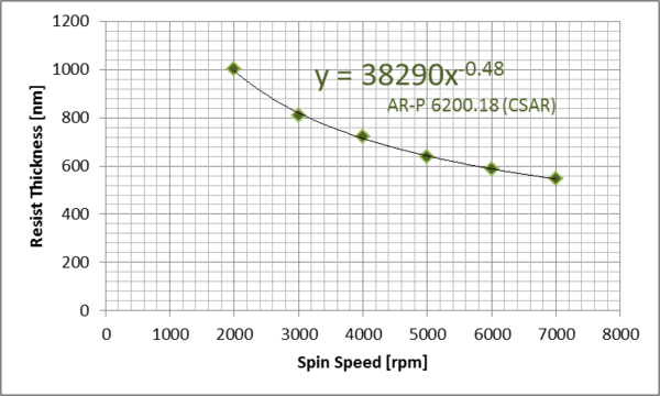
The thickness is measured on VASE Ellipsometer using a simple Cauchy model for a transparent polymer on Si. The measurements are performed at one incidence angle (70 degrees) only. 9 points on each 4" wafer has been measured; the standard deviation thus representing the homogeinity of the film on the 4" wafers. | |||
Around 2 ml of resist per wafer has been used when fabricating these curves. If you use less than 2 ml, the thickness of the final resist might be smaller than reported here. | |||
[[File:CSAR_09.png|right|600px]] | |||
[[File:CSAR_18.png|right|600px]] | |||
{|border="1" cellspacing="0" cellpadding="3" style="text-align:left;" style="width: 40%" | |||
|- | |- | ||
|- | |- | ||
|-style="background: | |-style="background:#00308F; color:White" | ||
! | !colspan="7"|AllResist AR-P 6200.09 (> 2ml per 4" wafer) spinning on Spin Coater: Manual LabSpin A-5, TIGRE, 09-04-2014. Softbake 5 min @ 150 degC. | ||
|- | |- | ||
|- | |- | ||
|-style="background: | |-style="background:silver; color:black" | ||
! | !Spin Speed [rpm] | ||
!Acceleration [1/s2] | |||
!Thickness [nm] | |||
|- | |- | ||
|- | |||
|-style="background:WhiteSmoke; color:black" | |||
|2000 | |||
|4000 | |||
|226 | |||
|- | |||
|- | |- | ||
|-style="background: | |-style="background:WhiteSmoke; color:black" | ||
| | |3000 | ||
|4000 | |||
| | |194 | ||
| | |||
|- | |- | ||
|- | |- | ||
|-style="background:WhiteSmoke; color:black | |-style="background:WhiteSmoke; color:black" | ||
|4000 | |||
|4000 | |||
|170 | |||
|- | |- | ||
|- | |||
|-style="background:WhiteSmoke; color:black" | |||
|5000 | |||
|4000 | |||
|151 | |||
|- | |||
|- | |- | ||
|-style="background: | |-style="background:WhiteSmoke; color:black" | ||
| | |6000 | ||
| | |4000 | ||
|142 | |||
| | |||
|- | |- | ||
|- | |- | ||
|-style="background:WhiteSmoke; color:black | |-style="background:WhiteSmoke; color:black" | ||
|7000 | |||
|4000 | |||
|127 | |||
|- | |- | ||
|} | |||
{|border="1" cellspacing="0" cellpadding="3" style="text-align:left;" style="width: 40%" | |||
|- | |- | ||
|-style="background: | |||
| | |- | ||
|-style="background:red; color:White" | |||
!colspan="7"|AllResist CSAR 6200.09 1:1 in anisole (< 2ml per 4" wafer), Spin Coater: Manual LabSpin A-5, TIGRE, 16-06-2014. Softbake 2 min @ 150 degC. | |||
|- | |- | ||
|- | |- | ||
|-style="background: | |-style="background:silver; color:black" style="text-align:left;" | ||
! | !Spin Speed [rpm] | ||
!Acceleration [1/s2] | |||
!Thickness [nm] | |||
|- | |- | ||
|- | |- | ||
|-style="background: | |-style="background:WhiteSmoke; color:black" | ||
| | |2000 | ||
| | |4000 | ||
|84 | |||
| | |||
|- | |- | ||
|- | |- | ||
|-style="background:WhiteSmoke; color:black | |-style="background:WhiteSmoke; color:black" | ||
|3000 | |||
|4000 | |||
|67 | |||
|- | |- | ||
|- | |- | ||
|-style="background: | |-style="background:WhiteSmoke; color:black" | ||
| | |4000 | ||
| | |4000 | ||
|59 | |||
| | |||
|- | |- | ||
|- | |- | ||
|-style="background:WhiteSmoke; color:black | |-style="background:WhiteSmoke; color:black" | ||
|5000 | |||
|4000 | |||
|53 | |||
|- | |- | ||
|- | |- | ||
|-style="background: | |-style="background:WhiteSmoke; color:black" | ||
| | |6000 | ||
| | |4000 | ||
| | |49 | ||
|- | |- | ||
|} | |} | ||
{|border="1" cellspacing="0" cellpadding="3" style="text-align:left;" style="width: 40%" | |||
{|border="1" cellspacing="0" cellpadding="3" style="text-align:left;" | |||
|- | |- | ||
|- | |- | ||
|-style="background: | |-style="background:green; color:White" | ||
!colspan="7"|AllResist | !colspan="7"|AllResist CSAR 6200.18 (< 2ml per 4" wafer), Spin Coater: Manual Standard Resists, E-5, TIGRE, 15-06-2016. Softbake 2 min @ 180 degC. | ||
|- | |- | ||
|- | |- | ||
|-style="background:silver; color:black" | |-style="background:silver; color:black" style="text-align:left;" | ||
!Spin Speed [rpm] | !Spin Speed [rpm] | ||
!Acceleration [1/s2] | !Acceleration [1/s2] | ||
!Thickness [nm] | !Thickness [nm] | ||
|- | |- | ||
| Line 131: | Line 152: | ||
|-style="background:WhiteSmoke; color:black" | |-style="background:WhiteSmoke; color:black" | ||
|2000 | |2000 | ||
| | |2000 | ||
| | |1003 | ||
|- | |- | ||
| Line 139: | Line 159: | ||
|-style="background:WhiteSmoke; color:black" | |-style="background:WhiteSmoke; color:black" | ||
|3000 | |3000 | ||
| | |2000 | ||
| | |809 | ||
|- | |- | ||
| Line 147: | Line 166: | ||
|-style="background:WhiteSmoke; color:black" | |-style="background:WhiteSmoke; color:black" | ||
|4000 | |4000 | ||
| | |2000 | ||
| | |721 | ||
|- | |- | ||
| Line 155: | Line 173: | ||
|-style="background:WhiteSmoke; color:black" | |-style="background:WhiteSmoke; color:black" | ||
|5000 | |5000 | ||
| | |2000 | ||
| | |639 | ||
|- | |- | ||
| Line 163: | Line 180: | ||
|-style="background:WhiteSmoke; color:black" | |-style="background:WhiteSmoke; color:black" | ||
|6000 | |6000 | ||
| | |2000 | ||
| | |586 | ||
|- | |- | ||
| Line 171: | Line 187: | ||
|-style="background:WhiteSmoke; color:black" | |-style="background:WhiteSmoke; color:black" | ||
|7000 | |7000 | ||
| | |2000 | ||
| | |549 | ||
|- | |- | ||
|} | |} | ||
<br> | |||
<br> | |||
<br> | |||
== Contrast Curve == | |||
=== CSAR 6200.09 === | |||
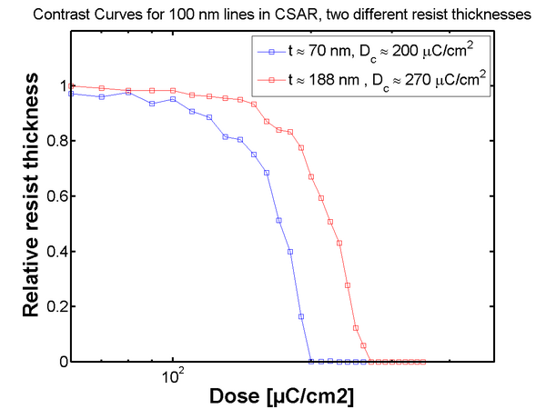
100 nm lines in both ~70 nm and ~188 nm thick CSAR has been developed with AR-600-546 (standard CSAR developer) at room temperature to provide the following contrast curves. | |||
{|border="1" cellspacing="0" cellpadding="3" style="text-align:left;" style="width: 95%" | |||
|- | |||
|- | |||
|-style="background:Black; color:White" | |||
!colspan="5"|CSAR Contrast Curve, Processed by TIGRE, FEB-MARCH 2016 | |||
|- | |||
|- | |- | ||
|-style="background:WhiteSmoke; color:black" | |||
!Resist | |||
!Spin Coat | |||
!E-beam exposure | |||
!Development | |||
!Characterisation | |||
|- | |||
|- | |||
|-style="background:WhiteSmoke; color:black" | |||
|CSAR AR-P6200.09 AllResist, CSAR AR-P6200.09 diluted 1:1 in Anisole | |||
|08-02-2016, LabSpin E-5, 4000 rpm, 60s, softbaked 60s @ 205 degC | |||
|09-02-2016, JBX9500 E-2, 2nA aperture 5, doses 40-600 µC/cm2, 100 nm lines and 300 nm spaces | |||
|11-02-2016, Fumehood D-2, AR-600-546, rinsed in IPA 60s. | |||
|02-03-2016 AFM Icon, F-2, ScanAsyst in Air | |||
|- | |||
|} | |||
{| style="border: none; border-spacing: 0; margin: 1em auto; text-align: center;" | |||
|- | |||
| [[image:ContrastCurvesCSAR_March2016_log.png|600px]] | |||
|- | |||
| colspan="1" style="text-align:center;| | |||
AR-P 6200 contrast curves. | |||
|} | |||
==Dose to size== | |||
Small features need a comparatively higher dose then big features and hence it can be useful to map out the dose and size dependency. Below is a set of cross sectional images of 100, 50 and 20 nm lines written 500, 250 and 180 nm resist at doses from 200 to 600 µC/cm<sup>2</sup>. | |||
{| style="border: none; border-spacing: 0; margin: 1em auto; text-align: center;" | |||
|- | |||
| [[image:thope240214_lines_100_06.png|1200px]] | |||
|- | |||
| [[image:thope240214_lines_50_11.png|1200px]] | |||
|- | |||
| [[image:thope240214_lines_20_13.png|1200px]] | |||
|- | |||
| colspan="1" style="text-align:center;| | |||
Cross section SEM images of 500 nm AR-P 6200.09 exposed at 200-600 µC/cm<sup>2</sup>. Top image is 100 nm lines, center image is 50 nm lines, bottom image is 20 nm lines. Au coated for SEM imaging. | |||
|} | |||
{| style="border: none; border-spacing: 0; margin: 1em auto; text-align: center;" | |||
|- | |- | ||
|- | | [[image:thope240214_lines250_100nm.png|1200px]] | ||
|- | |||
| [[image:thope240214_lines250_50nm.png|1200px]] | |||
|- | |||
| [[image:thope240214_lines250_20nm.png|1200px]] | |||
|- | |- | ||
| colspan="1" style="text-align:center;| | |||
Cross section SEM images of 250 nm AR-P 6200.09 exposed at 200-600 µC/cm<sup>2</sup>. Top image is 100 nm lines, center image is 50 nm lines, bottom image is 20 nm lines. Au coated for SEM imaging. | |||
|} | |||
{| style="border: none; border-spacing: 0; margin: 1em auto; text-align: center;" | |||
|- | |- | ||
|- | | [[image:thope240214_lines180_100_29.png|1200px]] | ||
|- | |||
| [[image:thope240214_lines180_50_31.png|1200px]] | |||
|- | |||
| [[image:thope240214_lines180_20_33.png|1200px]] | |||
|- | |||
| colspan="1" style="text-align:center;| | |||
Cross section SEM images of 180 nm AR-P 6200.09 exposed at 200-600 µC/cm<sup>2</sup>. Top image is 100 nm lines, center image is 50 nm lines, bottom image is 20 nm lines. Au coated for SEM imaging. | |||
|} | |||
=== CSAR 6200.18 === | |||
100 nm lines in ~900 nm thick CSAR has been developed with AR-600-546 (standard CSAR developer) at room temperature. | |||
[[File:CSAR 6200.18 developed with AR600546.png|right|400px]] | |||
{|border="1" cellspacing="0" cellpadding="3" style="text-align:right;" style="width: 60%" | |||
|- | |- | ||
|- | |- | ||
|-style="background: | |-style="background:Black; color:White" | ||
| | !colspan="5"|CSAR Contrast Curve, Processed by TIGRE, JUNE 2016 | ||
|- | |- | ||
|- | |- | ||
|-style="background:WhiteSmoke; color:black" | |-style="background:WhiteSmoke; color:black" | ||
!Resist | |||
!Spin Coat | |||
!E-beam exposure | |||
!Development | |||
!Characterisation | |||
|- | |- | ||
|- | |- | ||
|-style="background:WhiteSmoke; color:black" | |-style="background:WhiteSmoke; color:black" | ||
| | |CSAR AR-P6200.18 AllResist | ||
| | |15-06-2016, LabSpin E-5, 2000 rpm, 60s, softbaked 60s @ 205 degC | ||
| | |15-06-2016, JBX9500 E-2, 2nA aperture 5, doses 40-600 µC/cm2, 100 nm lines and 300 nm spaces | ||
| | |16-06-2016, Fumehood E-4, AR-600-546, 30s/60s/90s, rinsed in IPA 60s. | ||
|JUNE/JULY 2016 SEM Supra 2, 10 keV | |||
|- | |- | ||
|} | |||
<br clear="all"/> | |||
=== Dark Erosion === | |||
Dark erosion has been measured on a un-exposed 4" wafer spin coated with CSAR 6200.18 to a thickness of approximately 549 nm. The resist thickness has been measured by VASE Ellipsometer before development, and after 3 minutes, 13 minutes, and 30 minutes of development in AR 600 546. | |||
The graphs shows the measured thicknesses; the errorbars represents the standard deviations from the ellipsometric measurements. The average etch rate of CSAR is ~0.1 nm/min. | |||
[[File:dark erosion.png|right|400px]] | |||
<br clear="all" /> | |||
== Development == | |||
Many resists can be developed in different developers, CSAR can be developed in: AR 600-546, AR 600-548, ZED N-50 and mix of MIBK and IPA among others. | |||
CSAR and ZEP520A are in principle the same chemical, however the pretreatment (filtration and temperature control) can differ. | |||
Some users have reported residues and residual layers when using ZED N-50 on CSAR and vice verca, hence we recommend to use AR 600-546 or AR 600-548 (3 times stronger) to develop CSAR and not ZED N-50. | |||
When this is said some users still observe residues when using AR 600-546, the producer "'''All resist GMBH'''" have recommended to use 3-5s, dip in pure MIBK to remove residues. | |||
AR 600 546 will dissolve different plastic materials, hence never use it on PS compounds. | |||
<br clear="all"/> | |||
== Etch Tests == | |||
If you have wafers or chips with CSAR you would like to have tested, please send me an [[mailto:tigre@danchip.dtu.dk email]]. | |||
=== Chlorine versus flourine-based etches === | |||
We have experienced problems with removal of CSAR after chlorine-based dry etch, see the file [[:File:DryEtchTestsCSAR.pdf]]. It seems the chlorine etch forms particles of chlorinated CSAR on the surface, and these particles remains on the surface after resist removal with AR-600-71. The C4F8/SF6 etch also forms particles on the surface, but much smaller than those formed in the chlorine etch. It seems these particles are removed after 3 minutes in AR-600-71. | |||
=== How to mount chips in dry etch tools === | |||
All etch rates presented here are measured on chips (i.e. diced 4" wafers) crystal bonded to a carrier. The carrier is either a blank Si wafer, a Si wafer spin coated with resist or a Si wafer coated with ALD grown Al2O3. | |||
{|border="1" cellspacing="0" cellpadding="3" style="text-align:left;" style="width: 40%;" | |||
|- | |||
|+style="background:Black; color:White" colspan="4"|'''Etch Tests of CSAR, recipe 'nano1.42', DRIE PEGASUS, A-1. CSAR thickness measured on Ellipsometer VASE at 70 degrees''' | |||
|- | |||
|- | |||
!rowspan="1"|Sample | |||
!colspan="1"|CSAR Etch rate nm/min | |||
|- | |||
|Full 4" Si wafer with non-patterned ~180 nm CSAR | |||
|~56.5 (based on 2 runs) | |||
|- | |||
|- | |||
|Full 4" Si wafer with non-patterned ~240 nm CSAR, <br>postbaked 60 sec @ 130 degC | |||
|~56.5 (based on 2 runs) | |||
|- | |||
|- | |||
|1/4 4" Si wafer with non-patterned ~125 nm CSAR, <br>not crystal bonded to Si carrier | |||
|~83.3 (based on 3 runs) | |||
|- | |||
|- | |||
|1/4 4" Si wafer with non-patterned ~125 CSAR, <br>crystal bonded to 4" Si carrier | |||
|~54 (based on 1 run) | |||
|- | |||
|} | |} | ||
{|border="1" cellspacing="0" cellpadding="3" style="text-align:left;" | === Etch rates and profile inspection === | ||
==== Continous Etches ==== | |||
{|border="1" cellspacing="0" cellpadding="3" style="text-align:left;" style="width: 80%;" | |||
|- | |||
|+style="background:Black; color:White" colspan="4"|'''Recipe nano1.42 on Deep Reactive Ion Etch PEGASUS A-1''' | |||
|- | |||
|- | |||
! rowspan="4" align="center"| Recipe | |||
| Gasses | |||
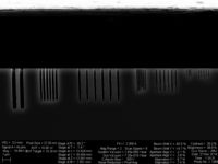
| C<sub>4</sub>F<sub>8</sub> 75 sccm, SF<sub>6</sub> 38 sccm | |||
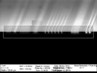
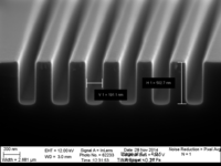
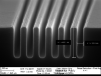
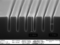
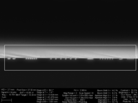
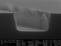
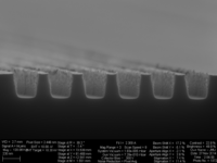
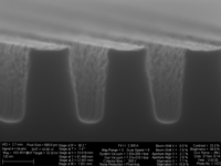
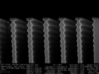
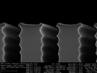
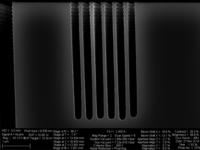
|rowspan="7" width="20%" | Profiles of lines exposed at 300 µC/cm2, etched 2:30 minutes (150s) with recipe 'nano1.42' | |||
[[File:617817 HD-4_11.png|200px]] [[File:617817 HD-4_18.png|200px]] | |||
[[File:617817 HD-4_16.png|200px]] [[File:617817 HD-4_14.png|200px]] | |||
|- | |- | ||
| Pressure | |||
| 4 mTorr, | |||
Strike: 3 secs @ 15 mTorr | |||
|- | |- | ||
| | | Power | ||
| 800 W Coil Power, | |||
40 W Platen Power | |||
|- | |||
|Platen temperature | |||
| - 20°C | |||
|- | |- | ||
! rowspan="1" align="center"| Conditions | |||
| Conditioning | |||
| Pre-clean: 10 min oxygen clean | |||
5 min oxygen clean between runs | |||
|- | |||
! rowspan="2" align="center"| Etch rates | |||
| Si | |||
| | |||
500 nm lines: ~200 nm/min <br> | |||
190 nm lines: ~200 nm/min <br> | |||
102 nm lines: ~190 nm/min <br> | |||
61 nm lines: ~170 nm/min | |||
|- | |- | ||
| | |CSAR | ||
| ~55 nm/min | |||
|- | |- | ||
|} | |||
{|border="1" cellspacing="0" cellpadding="3" style="text-align:left;" style="width: 80%;" | |||
|- | |||
|+style="background:Black; color:White" colspan="4"|'''Recipe processC on Deep Reactive Ion Etch PEGASUS A-1''' | |||
|- | |||
|- | |- | ||
! rowspan="4" align="center"| Recipe | |||
| | | Gasses | ||
| | | C<sub>4</sub>F<sub>8</sub> 70 sccm, SF<sub>6</sub> 38 sccm | ||
| | |rowspan="7" width="20%" | Profiles of lines exposed at 300 µC/cm2, etched 60s with recipe 'ProcessC' | ||
|0. | [[File:tigre 6.17 0% 3b_ 07.png|200px]] [[File:tigre 6.17 0% 3b_ 16.png|200px]] | ||
[[File:tigre 6.17 0% 3b_ 14.png|200px]] [[File:tigre 6.17 0% 3b_ 11.png|200px]] | |||
|- | |- | ||
| Pressure | |||
| 4 mTorr, | |||
Strike: secs @ mTorr | |||
|- | |- | ||
|- | | Power | ||
| | | 450 W Coil Power, 100 W Platen Power | ||
| | |- | ||
| | |Platen temperature | ||
| 10°C | |||
|- | |||
! rowspan="1" align="center"| Conditions | |||
| Conditioning | |||
| Pre-clean: 10 min oxygen clean | |||
5 min oxygen clean between runs | |||
|- | |- | ||
! rowspan="2" align="center"| Etch rates | |||
| Si | |||
| | |||
500 nm lines: ~300 nm/min <br> | |||
102 nm lines: ~250 nm/min <br> | |||
|- | |- | ||
| | |CSAR | ||
| | | 158 nm/min | ||
|- | |- | ||
|} | |||
==== Bosch Etch ==== | |||
{|border="1" cellspacing="0" cellpadding="3" style="text-align:left;" style="width: 80%;" | |||
|- | |||
|+style="background:Black; color:White" colspan="4"|'''Recipe NBoost01 on Deep Reactive Ion Etch PEGASUS A-1''' | |||
|- | |||
|- | |||
! rowspan="13" align="center" width ="70"| Recipe | |||
| rowspan="4" width ="50"| Deposition step | |||
|Duration | |||
| width ="100" |2.5 s | |||
|rowspan="16" width="20%" | Profiles of lines exposed at 300 µC/cm2, etched 6:00 minutes with recipe 'NBoost01' | |||
[[File:tigre 6.17 -15% 3a_ 11.png|200px]] [[File:tigre 6.17 3a_ 08.png|200px]] | |||
[[File:tigre 6.17 3a_ 20.png|200px]] [[File:tigre 6.17 3a_ 21.png|200px]] | |||
[[File:tigre 6.17 3a_ 22.png|200px]] | |||
|- | |||
| width ="30"| Gasses | |||
|C<sub>4</sub>F<sub>8</sub> 50 sccm, SF<sub>6</sub> 0 sccm | |||
|- | |||
| Pressure | |||
|10 mTorr | |||
|- | |||
| Powers | |||
|500 W Coil | |||
|- | |||
| rowspan="4"| Etch step (boost) | |||
|Duration | |||
|1.5 s | |||
|- | |||
| Gasses | |||
|C<sub>4</sub>F<sub>8</sub> 0 sccm, SF<sub>6</sub> 60 sccm | |||
|- | |||
| Pressure | |||
|5 mTorr | |||
|- | |- | ||
| | | Powers | ||
| | |400 W Coil, 50 W Platen | ||
|- | |- | ||
| rowspan="4"| Etch step (main) | |||
|Duration | |||
|3.5 s | |||
|- | |- | ||
|- | | Gasses | ||
| | |C<sub>4</sub>F<sub>8</sub> 40 sccm, SF<sub>6</sub> 60 sccm | ||
| | |- | ||
| | | Pressure | ||
| | |15 mTorr | ||
|- | |||
| Powers | |||
|400 W Coil, 20 W Platen | |||
|- | |||
|Platen temperature | |||
|colspan="2"|20 °C | |||
|- | |||
! rowspan="1" align="center"| Conditions | |||
| Conditioning | |||
|colspan="2"| Pre-clean: 10 min oxygen clean | |||
5 min oxygen clean between runs | |||
|- | |- | ||
! rowspan="2" align="center"| Etch rates | |||
| Si | |||
|colspan="2"| | |||
200 nm lines: ~700 nm/min <br> | |||
130 nm lines: ~580 nm/min <br> | |||
|- | |||
|CSAR | |||
|colspan="2"| ~18 nm/min | |||
|- | |||
|} | |} | ||
Latest revision as of 08:36, 21 February 2024
Simple e-beam pattern in this resist has been tested, the results showed on this page. If you have questions to the process or wish to use this e-beam resist, please contact lithography at DTU Nanolab.
Spin Curves
The thickness is measured on VASE Ellipsometer using a simple Cauchy model for a transparent polymer on Si. The measurements are performed at one incidence angle (70 degrees) only. 9 points on each 4" wafer has been measured; the standard deviation thus representing the homogeinity of the film on the 4" wafers.
Around 2 ml of resist per wafer has been used when fabricating these curves. If you use less than 2 ml, the thickness of the final resist might be smaller than reported here.
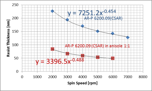
| AllResist AR-P 6200.09 (> 2ml per 4" wafer) spinning on Spin Coater: Manual LabSpin A-5, TIGRE, 09-04-2014. Softbake 5 min @ 150 degC. | ||||||
|---|---|---|---|---|---|---|
| Spin Speed [rpm] | Acceleration [1/s2] | Thickness [nm] | ||||
| 2000 | 4000 | 226 | ||||
| 3000 | 4000 | 194 | ||||
| 4000 | 4000 | 170 | ||||
| 5000 | 4000 | 151 | ||||
| 6000 | 4000 | 142 | ||||
| 7000 | 4000 | 127 | ||||
| AllResist CSAR 6200.09 1:1 in anisole (< 2ml per 4" wafer), Spin Coater: Manual LabSpin A-5, TIGRE, 16-06-2014. Softbake 2 min @ 150 degC. | ||||||
|---|---|---|---|---|---|---|
| Spin Speed [rpm] | Acceleration [1/s2] | Thickness [nm] | ||||
| 2000 | 4000 | 84 | ||||
| 3000 | 4000 | 67 | ||||
| 4000 | 4000 | 59 | ||||
| 5000 | 4000 | 53 | ||||
| 6000 | 4000 | 49 | ||||
| AllResist CSAR 6200.18 (< 2ml per 4" wafer), Spin Coater: Manual Standard Resists, E-5, TIGRE, 15-06-2016. Softbake 2 min @ 180 degC. | ||||||
|---|---|---|---|---|---|---|
| Spin Speed [rpm] | Acceleration [1/s2] | Thickness [nm] | ||||
| 2000 | 2000 | 1003 | ||||
| 3000 | 2000 | 809 | ||||
| 4000 | 2000 | 721 | ||||
| 5000 | 2000 | 639 | ||||
| 6000 | 2000 | 586 | ||||
| 7000 | 2000 | 549 | ||||
Contrast Curve
CSAR 6200.09
100 nm lines in both ~70 nm and ~188 nm thick CSAR has been developed with AR-600-546 (standard CSAR developer) at room temperature to provide the following contrast curves.
| CSAR Contrast Curve, Processed by TIGRE, FEB-MARCH 2016 | ||||
|---|---|---|---|---|
| Resist | Spin Coat | E-beam exposure | Development | Characterisation |
| CSAR AR-P6200.09 AllResist, CSAR AR-P6200.09 diluted 1:1 in Anisole | 08-02-2016, LabSpin E-5, 4000 rpm, 60s, softbaked 60s @ 205 degC | 09-02-2016, JBX9500 E-2, 2nA aperture 5, doses 40-600 µC/cm2, 100 nm lines and 300 nm spaces | 11-02-2016, Fumehood D-2, AR-600-546, rinsed in IPA 60s. | 02-03-2016 AFM Icon, F-2, ScanAsyst in Air |
|
|
AR-P 6200 contrast curves. |
Dose to size
Small features need a comparatively higher dose then big features and hence it can be useful to map out the dose and size dependency. Below is a set of cross sectional images of 100, 50 and 20 nm lines written 500, 250 and 180 nm resist at doses from 200 to 600 µC/cm2.

|

|

|
|
Cross section SEM images of 500 nm AR-P 6200.09 exposed at 200-600 µC/cm2. Top image is 100 nm lines, center image is 50 nm lines, bottom image is 20 nm lines. Au coated for SEM imaging. |

|

|

|
|
Cross section SEM images of 250 nm AR-P 6200.09 exposed at 200-600 µC/cm2. Top image is 100 nm lines, center image is 50 nm lines, bottom image is 20 nm lines. Au coated for SEM imaging. |

|

|

|
|
Cross section SEM images of 180 nm AR-P 6200.09 exposed at 200-600 µC/cm2. Top image is 100 nm lines, center image is 50 nm lines, bottom image is 20 nm lines. Au coated for SEM imaging. |
CSAR 6200.18
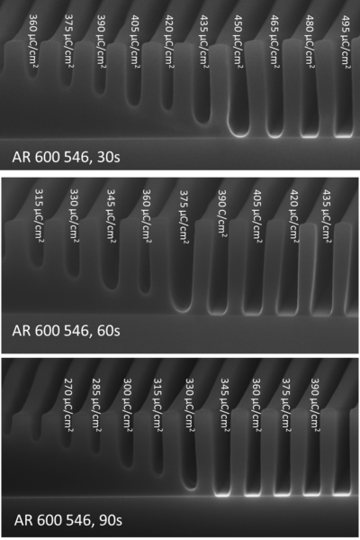
100 nm lines in ~900 nm thick CSAR has been developed with AR-600-546 (standard CSAR developer) at room temperature.
| CSAR Contrast Curve, Processed by TIGRE, JUNE 2016 | ||||
|---|---|---|---|---|
| Resist | Spin Coat | E-beam exposure | Development | Characterisation |
| CSAR AR-P6200.18 AllResist | 15-06-2016, LabSpin E-5, 2000 rpm, 60s, softbaked 60s @ 205 degC | 15-06-2016, JBX9500 E-2, 2nA aperture 5, doses 40-600 µC/cm2, 100 nm lines and 300 nm spaces | 16-06-2016, Fumehood E-4, AR-600-546, 30s/60s/90s, rinsed in IPA 60s. | JUNE/JULY 2016 SEM Supra 2, 10 keV |
Dark Erosion
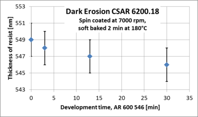
Dark erosion has been measured on a un-exposed 4" wafer spin coated with CSAR 6200.18 to a thickness of approximately 549 nm. The resist thickness has been measured by VASE Ellipsometer before development, and after 3 minutes, 13 minutes, and 30 minutes of development in AR 600 546.
The graphs shows the measured thicknesses; the errorbars represents the standard deviations from the ellipsometric measurements. The average etch rate of CSAR is ~0.1 nm/min.
Development
Many resists can be developed in different developers, CSAR can be developed in: AR 600-546, AR 600-548, ZED N-50 and mix of MIBK and IPA among others.
CSAR and ZEP520A are in principle the same chemical, however the pretreatment (filtration and temperature control) can differ.
Some users have reported residues and residual layers when using ZED N-50 on CSAR and vice verca, hence we recommend to use AR 600-546 or AR 600-548 (3 times stronger) to develop CSAR and not ZED N-50.
When this is said some users still observe residues when using AR 600-546, the producer "All resist GMBH" have recommended to use 3-5s, dip in pure MIBK to remove residues.
AR 600 546 will dissolve different plastic materials, hence never use it on PS compounds.
Etch Tests
If you have wafers or chips with CSAR you would like to have tested, please send me an [email].
Chlorine versus flourine-based etches
We have experienced problems with removal of CSAR after chlorine-based dry etch, see the file File:DryEtchTestsCSAR.pdf. It seems the chlorine etch forms particles of chlorinated CSAR on the surface, and these particles remains on the surface after resist removal with AR-600-71. The C4F8/SF6 etch also forms particles on the surface, but much smaller than those formed in the chlorine etch. It seems these particles are removed after 3 minutes in AR-600-71.
How to mount chips in dry etch tools
All etch rates presented here are measured on chips (i.e. diced 4" wafers) crystal bonded to a carrier. The carrier is either a blank Si wafer, a Si wafer spin coated with resist or a Si wafer coated with ALD grown Al2O3.
| Sample | CSAR Etch rate nm/min |
|---|---|
| Full 4" Si wafer with non-patterned ~180 nm CSAR | ~56.5 (based on 2 runs) |
| Full 4" Si wafer with non-patterned ~240 nm CSAR, postbaked 60 sec @ 130 degC |
~56.5 (based on 2 runs) |
| 1/4 4" Si wafer with non-patterned ~125 nm CSAR, not crystal bonded to Si carrier |
~83.3 (based on 3 runs) |
| 1/4 4" Si wafer with non-patterned ~125 CSAR, crystal bonded to 4" Si carrier |
~54 (based on 1 run) |
Etch rates and profile inspection
Continous Etches

