Specific Process Knowledge/Characterization/AFM: Atomic Force Microscopy: Difference between revisions
mNo edit summary |
|||
| (33 intermediate revisions by 3 users not shown) | |||
| Line 4: | Line 4: | ||
=AFM Icon 1 & 2 = | =AFM Icon 1 & 2 = | ||
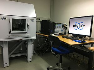
[[Image:P6180008.JPG|right|thumb|300px| AFM Icon-Pt Positioned in clean room: C-1]] | ''This section is written by Berit Herstrøm @DTU Nanolab | ||
[[Image:Foto of system in basement.jpg|right|thumb|300px| AFM Icon-Pt 2 Positioned in the basement of building 346-904]] | [[Image:P6180008.JPG|right|thumb|300px| AFM Icon-Pt Positioned in clean room: C-1, photo: DTU Nanolab internal]] | ||
[[Image:Foto of system in basement.jpg|right|thumb|300px| AFM Icon-Pt 2 Positioned in the basement of building 346-904, photo: DTU Nanolab internal]] | |||
DTU Nanolab has two pieces of Bruker AFM Dimension Icon-Pt. AFM stands for Atomic Force Microscope which is a scanning probe microscope where a sharp probe is scanned across a surface either in contact mode, tapping mode or PeakForce tapping mode. The outcome is a topographic plot of the surface. It has a lateral solution of about 1 nm and a vertical resolution of less than 1 Å which makes it very suitable for topographic characterization in the nanometer regime. The limiting factor however is often the size of the probe in use. The tip radius of curvature (ROC) can be from 2 nm up to more than 20 nm depending on the chosen probe. The half cone angle of the tip can vary from less than 3<sup>o</sup> to over 25<sup>o</sup> giving problems resolving high aspect ratio structures. | DTU Nanolab has two pieces of Bruker AFM Dimension Icon-Pt. AFM stands for Atomic Force Microscope which is a scanning probe microscope where a sharp probe is scanned across a surface either in contact mode, tapping mode or PeakForce tapping mode. The outcome is a topographic plot of the surface. It has a lateral solution of about 1 nm and a vertical resolution of less than 1 Å which makes it very suitable for topographic characterization in the nanometer regime. The limiting factor however is often the size of the probe in use. The tip radius of curvature (ROC) can be from 2 nm up to more than 20 nm depending on the chosen probe. The half cone angle of the tip can vary from less than 3<sup>o</sup> to over 25<sup>o</sup> giving problems resolving high aspect ratio structures. | ||
The main purposes are surface roughness measurements and step/structure high measurements in the nanometer and sub-micrometer regime. For larger structure see the [[Specific Process Knowledge/Characterization/Topographic measurement|topografic measurement]] page. | The main purposes are surface roughness measurements and step/structure high measurements in the nanometer and sub-micrometer regime. For larger structure see the [[Specific Process Knowledge/Characterization/Topographic measurement|topografic measurement]] page. | ||
To get some product information from the vendor take a look at Bruker's homepage [ | To get some product information from the vendor take a look at Bruker's homepage [https://www.bruker.com/en/products-and-solutions/microscopes/materials-afm/dimension-icon-afm.html] | ||
| Line 19: | Line 20: | ||
AFM Icon Part 3 | AFM Icon Part 3 | ||
You can find them here: [ | You can find them here: [https://www.youtube.com/playlist?list=PLjWVU97LayHC9xeoG2uv8IaHuY7t-q0Tj link to training videos] | ||
It is also recommanded to read | It is also recommanded to read this presentation of contract mode, tapping mode and peak force tapping mode [https://labmanager.dtu.dk/view_binary.php?fileId=5383 click HERE - requires login] | ||
| Line 35: | Line 36: | ||
[[Image:Nanoman cantilever AR5.jpg|right|thumb|AR5-NCHR tip<br /> (Aspect Ratio 5)]] | [[Image:Nanoman cantilever AR5.jpg|right|thumb|AR5-NCHR tip<br /> (Aspect Ratio 5)]] | ||
--> | --> | ||
*[https://labmanager.dtu.dk/view_binary.php?fileId=5383 Introduction to contact mode, tapping mode and peak force tapping mode + how to improve image quality- requires login] | |||
* | |||
*[[/AFM Icon Acceptance|AFM Icon Acceptance 1 & 2 and overview of accessories and modes on the systems]] | *[[/AFM Icon Acceptance|AFM Icon Acceptance 1 & 2 and overview of accessories and modes on the systems]] | ||
*[[/Workspaces|What experiment/mode and probe to select]] | *[[/Workspaces|What experiment/mode and probe to select]] | ||
*[[/KPFM|KPFM measurements - work function]] | *[[/KPFM|KPFM measurements - work function]] | ||
===Analysis software=== | |||
*Free analysis software: For visualizing and analyzing AFM and Optical profiler files (Nanoman and Sensofar) [http://gwyddion.net Gwyddion] | |||
*or you can install Brukers own software analyses program that can be found on the cleanroom drive: U:\Nlab\CleanroomDrive\_Equipment\AFM\NanoScope_Analysis_x86_v170r1sr2.exe | |||
*or you can get a SPIP license for free if you are connected to one of the following institutes (Nanolab, Physics, Chemistry, Mechanics, Energikonvertering, this list may not be updated!). | |||
==An overview of the performance of the AFM Icon== | ==An overview of the performance of the AFM Icon== | ||
| Line 115: | Line 112: | ||
|style="background:WhiteSmoke; color:black"|<0.15nm RMS | |style="background:WhiteSmoke; color:black"|<0.15nm RMS | ||
|style="background:WhiteSmoke; color:black"|<0.15nm RMS | |style="background:WhiteSmoke; color:black"|<0.15nm RMS | ||
|- | |||
|style="background:silver; color:black"| | |||
|style="background:LightGrey; color:black"|[[#Height Accuracy|Height (z) accuracy]] | |||
|style="background:WhiteSmoke; color:black"|better than 2% (at 200 nm), typically better then 0.75% | |||
|style="background:WhiteSmoke; color:black"|better than 2% (at 200 nm), typically better then 0.75% | |||
|- | |- | ||
|style="background:silver; color:black"| | |style="background:silver; color:black"| | ||
| Line 185: | Line 187: | ||
<br clear="all" /> | <br clear="all" /> | ||
===Height Accuracy=== | |||
Height accuracy estimations in AFM measurements are complex and depends on the scale you are interested in. At sub nanometer scale or a few nanometers the height measurement may be affected by the properties of the cantilever tip, your sample material stiffness and the scanning force. These parameters are less important when measuring in the 100 nm range and above. At all scales calibration of the Z-piezo is important. | |||
Here at DTU Nanolab we calibrate the Z-piezo with a certified sample that is approximately 200 nm in height. This sample height is given with an uncertainty that is calculated based on variation on the calibration sample and measurement uncertainties of the instrument used for certification. The uncertainty on the calibration sample is ≤ 1.5 nm. Following our QC procedure we accept an offset from the certified value of 2%. For a 200 nm sample this is 4 nm. If we use the formula for combined uncertainties then the uncertainty is: 4.3 nm or 2.1% | |||
However when we check the value it is typically less then 1% off given a combined uncertainty of: 0.75% | |||
===Tip status=== | |||
''This section is written by Jesper Pan @DTU Nanolab | |||
[[Image:section under construction.jpg|150px]] | |||
When measuring a sample using an AFM, the resulting image is the convolution of the tip shape and sample shape. | |||
As the tip is worn, it will become less sharp, thus the resulting image will look blurry. | |||
This effect is especially visible when imaging samples with sharp/edged features, and drastically change roughness parameters like R<sub>max</sub>, R<sub>q</sub> and R<sub>a</sub>. Therefore it is important to be able to identify a worn tip. | |||
The figure below shows a comparison of the [https://www.budgetsensors.com/sample-for-tip-evaluation-tipcheck link TipCheck sample]. | |||
The left image shows a worm tip scanning across a rough surface with sharp edges. Due to tip convolution you practically use the sample to measure the shape of the tip. In this case, the tip is an oval pointing towards the top left, which causes all features to look like that. Furthermore, the worn tip is too big to reach bottom of the trenches between the structures. Which result in a lower measured roughness and Z-range. | |||
{| class="wikitable" style="max-width:800px" | |||
|+ Comparison between images of the Tip Checker sample | |||
|- | |||
! !! Worn Probe !! New probe | |||
|- | |||
! Image | |||
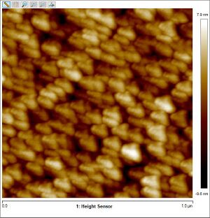
| [[File:AFMWornTip.jpg|thumb|left|alt=Image taken using a worn probe| AFM image of the tip checker sample taken using a worn AFM probe]] | |||
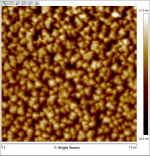
| [[File:AFMNewTip.jpg|thumb|left|alt=Image taken using a new probe| AFM image of the tip checker sample taken using a new AFM probe]] | |||
|- | |||
! Image Parameters and | |||
Roughness information | |||
| | |||
* Scan mode: PeakForce Tapping | |||
* Probe: Tap 150Al | |||
* Size: 1µm | |||
* Scan Speed: 1Hz | |||
---- | |||
* R<sub>q</sub>: 2.49 nm | |||
* R<sub>a</sub>: 1.97 nm | |||
* R<sub>max</sub>: 18.8 nm | |||
| | |||
* Scan mode: PeakForce Tapping | |||
* Probe: Tap 150Al | |||
* Size: 1µm | |||
* Scan Speed: 1Hz | |||
---- | |||
* R<sub>q</sub>: 10.5 nm | |||
* R<sub>a</sub>: 8.45 nm | |||
* R<sub>max</sub>: 78.3 nm | |||
|- | |||
! Comments | |||
| The shape of the probe causes all features to look like an oval pointing towards the top left of the image. Low measured roughness as the worn tip skates across the top of the triangles. | |||
| Same sample taken with a new probe. The triangular structures are pointing in different directions. Higher measured roughness as the sharper tip can map the trenches between the triangles. | |||
|} | |||
===Tip Wear=== | |||
''This section is written by Jesper Pan @DTU Nanolab | |||
[[Image:section under construction.jpg|150px]] | |||
Section about degradation of the tip as you continue scanning | |||
Latest revision as of 11:38, 6 February 2024
Feedback to this page: click here
AFM Icon 1 & 2
This section is written by Berit Herstrøm @DTU Nanolab


DTU Nanolab has two pieces of Bruker AFM Dimension Icon-Pt. AFM stands for Atomic Force Microscope which is a scanning probe microscope where a sharp probe is scanned across a surface either in contact mode, tapping mode or PeakForce tapping mode. The outcome is a topographic plot of the surface. It has a lateral solution of about 1 nm and a vertical resolution of less than 1 Å which makes it very suitable for topographic characterization in the nanometer regime. The limiting factor however is often the size of the probe in use. The tip radius of curvature (ROC) can be from 2 nm up to more than 20 nm depending on the chosen probe. The half cone angle of the tip can vary from less than 3o to over 25o giving problems resolving high aspect ratio structures.
The main purposes are surface roughness measurements and step/structure high measurements in the nanometer and sub-micrometer regime. For larger structure see the topografic measurement page.
To get some product information from the vendor take a look at Bruker's homepage [1]
Before training: Please watch the training videos before the training on the instrument:
AFM Icon Part 1, AFM Icon Part 2 and AFM Icon Part 3
You can find them here: link to training videos
It is also recommanded to read this presentation of contract mode, tapping mode and peak force tapping mode click HERE - requires login
The user manual, quality control procedure and results and contact information can be found in LabManager:
AFM Icon 1 in LabManager
AFM Icon 2 in LabManager
Process Information
- Introduction to contact mode, tapping mode and peak force tapping mode + how to improve image quality- requires login
- AFM Icon Acceptance 1 & 2 and overview of accessories and modes on the systems
- What experiment/mode and probe to select
- KPFM measurements - work function
Analysis software
- Free analysis software: For visualizing and analyzing AFM and Optical profiler files (Nanoman and Sensofar) Gwyddion
- or you can install Brukers own software analyses program that can be found on the cleanroom drive: U:\Nlab\CleanroomDrive\_Equipment\AFM\NanoScope_Analysis_x86_v170r1sr2.exe
- or you can get a SPIP license for free if you are connected to one of the following institutes (Nanolab, Physics, Chemistry, Mechanics, Energikonvertering, this list may not be updated!).
An overview of the performance of the AFM Icon
| Equipment | AFM Icon | AFM Icon 2 | |
|---|---|---|---|
| Position |
Inside the cleanroom |
In the basement of building 346 room 904 | |
| Purpose | Topografic measurement in the nanometer and and sub-micrometer regime and electrical and mechanical measurements |
|
|
| Performance | Scan range xy | Up to 90 µm square | Up to 90 µm square |
| Scan range z | Up to 13µm | Up to 13µm | |
| Vertical noise floor | <30pm RMS | <30pm RMS | |
| X-Y position noise (closed loop) | <0.15nm RMS | <0.15nm RMS | |
| Z sensor noise level(closed loop) | 35pm RMS | 35pm RMS | |
| Integral nonlinearity(X-Y-Z) | <0.5% | <0.5% | |
| X-Y position noise (closed loop) | <0.15nm RMS | <0.15nm RMS | |
| Height (z) accuracy | better than 2% (at 200 nm), typically better then 0.75% | better than 2% (at 200 nm), typically better then 0.75% | |
| Max. scan depth as a function of trench width W | ~1 for our standard probe. Can be improved to about 10 with the right probe | ~1 for our standard probe. Can be improved to about 10 with the right probe | |
| Hardware settings | Tip radius of curvature | Standard probe: <12 nm | Standard probe: <12 nm |
| Standard soft tapping mode Cantilever/tip (can be used in both tapping mode and ScanAsyst mode) | Tap150Al-G | Tap150Al-G | |
| Standard ScanAsyst mode Cantilever/tip | ScanAsyst in Air | ScanAsyst in Air | |
| Standard Tapping mode Cantilevers/tips | Tap300Al-G | Tap300Al-G | |
| Super Sharp Si Cantilever/tip | SSS-NCHR | SSS-NCHR | |
| High Aspect Ratio Cantilever/tip | AR5-NCHR | AR5-NCHR | |
| Cantilevers/tips vendor | |||
| Substrates | Substrate size | Up to 210mm in diameter and up to 15mm thick" | Up to 210mm in diameter and up to 15mm thick" |
| Motorized stage (X-Y axis) |
|
| |
| Substrate material allowed | In principle all solid and none-poisonous materials | In principle all solid and none-poisonous materials | |
Height Accuracy
Height accuracy estimations in AFM measurements are complex and depends on the scale you are interested in. At sub nanometer scale or a few nanometers the height measurement may be affected by the properties of the cantilever tip, your sample material stiffness and the scanning force. These parameters are less important when measuring in the 100 nm range and above. At all scales calibration of the Z-piezo is important.
Here at DTU Nanolab we calibrate the Z-piezo with a certified sample that is approximately 200 nm in height. This sample height is given with an uncertainty that is calculated based on variation on the calibration sample and measurement uncertainties of the instrument used for certification. The uncertainty on the calibration sample is ≤ 1.5 nm. Following our QC procedure we accept an offset from the certified value of 2%. For a 200 nm sample this is 4 nm. If we use the formula for combined uncertainties then the uncertainty is: 4.3 nm or 2.1% However when we check the value it is typically less then 1% off given a combined uncertainty of: 0.75%
Tip status
This section is written by Jesper Pan @DTU Nanolab

When measuring a sample using an AFM, the resulting image is the convolution of the tip shape and sample shape. As the tip is worn, it will become less sharp, thus the resulting image will look blurry. This effect is especially visible when imaging samples with sharp/edged features, and drastically change roughness parameters like Rmax, Rq and Ra. Therefore it is important to be able to identify a worn tip.
The figure below shows a comparison of the link TipCheck sample. The left image shows a worm tip scanning across a rough surface with sharp edges. Due to tip convolution you practically use the sample to measure the shape of the tip. In this case, the tip is an oval pointing towards the top left, which causes all features to look like that. Furthermore, the worn tip is too big to reach bottom of the trenches between the structures. Which result in a lower measured roughness and Z-range.
Tip Wear
This section is written by Jesper Pan @DTU Nanolab
 Section about degradation of the tip as you continue scanning


