Specific Process Knowledge/Etch/ICP Metal Etcher/silicon oxide: Difference between revisions
| (19 intermediate revisions by 2 users not shown) | |||
| Line 1: | Line 1: | ||
'''Feedback to this page''': '''[mailto:labadviser@ | '''Feedback to this page''': '''[mailto:labadviser@nanolab.dtu.dk?Subject=Feed%20back%20from%20page%20http://labadviser.nanolab.dtu.dk/index.php/Specific_Process_Knowledge/Etch/ICP_Metal_Etcher/silicon_oxide click here]''' | ||
<br> {{CC-bghe1}} | |||
It is possible to etch SiO2 in the ICP metal etcher but it is not designed for it and | =SiO2 etching in the ICP metal= | ||
It is possible to etch SiO2 in the ICP metal etcher but it is not designed for it and we prefer that you do it elsewhere. It is a challenge to get a good selectivity to resist (typically in the range of 1:1 or worse) and it is probably not possible to get a profile angle of 90 degrees. More likely about 75-85 degrees. Different chemistries can be applied either based on CF4 or C4F8. If seems that C4F8 can give the best selectivity to resist (best case I have seem was 1:11 but it depends a lot on the process parameters)). If low coil power is needed CF4 chemistry is used because C4F8 needs a higher power to generate a plasma. ''/bghe 2016-04-25 '' | |||
==Slow etch of SiO2 with resist as masking material - using a 6" carrier wafer with recess == | ==Slow etch of SiO2 with resist as masking material - using a 6" carrier wafer with recess == | ||
| Line 35: | Line 37: | ||
|-style="background:Black; color:White" | |-style="background:Black; color:White" | ||
!Results | !Results | ||
!Test on wafer with 50% load (Travka 50), by BGHE @ | !Test on wafer with 50% load (Travka 50), by BGHE @nanolab | ||
!100% load on 100mm wafers with Barc and KRF (no mask) | !100% load on 100mm wafers with Barc and KRF (no mask) | ||
|- | |- | ||
| Line 45: | Line 47: | ||
|'''~0.9''' (SiO2:resist) | |'''~0.9''' (SiO2:resist) | ||
|'''~1.25:1 (Barc:KRF) | |'''~1.25:1 (Barc:KRF) | ||
|- | |||
|Etch rate in silicon | |||
| | |||
bghe@Nanolab 20190117 | |||
*33.8 nm/min (middle of wafer with 80% load) bghe@Nanolab 20190117 | |||
*34.3 nm/min (edge of wafer with 80% load) | |||
| | |||
|- | |- | ||
|Wafer uniformity (100mm) | |Wafer uniformity (100mm) | ||
| Line 86: | Line 95: | ||
*[[/By Peixiong|Tests done by Peixiong]] | *[[/By Peixiong|Tests done by Peixiong]] | ||
*[[/By BGHE|Tests done by Berit]] | *[[/By BGHE|Tests done by Berit]] | ||
*Test by Zhibo Li @ | *Test by Zhibo Li @nanolab ''dec. 2016'' - based on the work of Peixiong and Berit: [[:File:Zhibo Li SiO2 ICP etch (dose205).docx]] | ||
<br/> | <br/> | ||
{| border="2" cellspacing="2" cellpadding="3" | {| border="2" cellspacing="2" cellpadding="3" | ||
|-style="background:Gray; color:White" | |-style="background:Gray; color:White" | ||
!Parameter | !Parameter | ||
!Recipe on ICP metal: A SiO2 etch with C4F8 with resist mask | !Recipe on ICP metal: A SiO2 etch with C4F8 with resist mask | ||
|- | |- | ||
|Coil Power [W] | |Coil Power [W] | ||
|1000 | |1000 | ||
|- | |- | ||
|Platen Power [W] | |Platen Power [W] | ||
|200 | |200 | ||
|- | |- | ||
|Platen temperature [<sup>o</sup>C] | |Platen temperature [<sup>o</sup>C] | ||
|0 | |0 | ||
|- | |- | ||
|C<sub>4</sub>F<sub>8</sub> flow [sccm] | |C<sub>4</sub>F<sub>8</sub> flow [sccm] | ||
|10 | |10 | ||
|- | |- | ||
|H<sub>2</sub> flow [sccm] | |H<sub>2</sub> flow [sccm] | ||
|28 | |28 | ||
|- | |- | ||
|Pressure [mTorr] | |Pressure [mTorr] | ||
|2.5 | |2.5 | ||
|- | |- | ||
| Line 125: | Line 127: | ||
|-style="background:Black; color:White" | |-style="background:Black; color:White" | ||
!Results | !Results | ||
!Test | !Test | ||
|- | |- | ||
|Etch rate of thermal oxide | |Etch rate of thermal oxide | ||
|'''145-172 nm/min''' ''by bghe@ | | | ||
*'''145-172 nm/min''' ''by bghe@nanolab (2015-06-02)'' | |||
*'''145 nm/min ''' ''by Martin Lind Ommen (fall 2016)'' | |||
|- | |- | ||
|Selectivity to resist [:1] | |Selectivity to resist [:1] | ||
| 4-5:1 (SiO2:resist) | | 4-5:1 (SiO2:resist) ''by bghe@nanolab (2015-06-02)'' | ||
|- | |- | ||
|Cr etch rate | |Cr etch rate | ||
|1.6 nm/min (1:90 to SiO2) ''by Martin Lind Ommen (fall 2016)'' | |1.6 nm/min (1:90 to SiO2) ''by Martin Lind Ommen (fall 2016)'' | ||
|- | |- | ||
|Profile [<sup>o</sup>] | |Profile [<sup>o</sup>] | ||
|86-87 dg | |86-87 dg ''by bghe@nanolab (2015-06-02)'' | ||
|- | |- | ||
|Wafer uniformity map (click on the image to view a larger image) | |Wafer uniformity map (click on the image to view a larger image) | ||
| | | | ||
|- | |- | ||
|SEM profile images | |SEM profile images | ||
| | |[[File:ICP metal s007592_21.jpg|200px]] [[File:ICP metal s007592_24.jpg|200px]]<br> ''by bghe@nanolab (2015-06-02)'' | ||
| | |||
|- | |- | ||
|Etch rate in barc | |Etch rate in barc | ||
| | | | ||
|- | |- | ||
|Etch rate in KRF resist | |Etch rate in KRF resist | ||
| | |34 nm/min ''by bghe@nanolab (2015-06-02)'' | ||
|- | |- | ||
|Comments | |Comments | ||
| | | | ||
*Sample: s007592 ''by bghe@nanolab (2015-06-02)'' | |||
*See Martin Lind Ommen's results with hard masks: [https://labadviser.nanolab.dtu.dk//index.php?title=Specific_Process_Knowledge/Etch/Etching_of_Silicon_Oxide#Dry_etch_with_Hard_mask] <br> There were problems with polymer on the surface after etching. | |||
|} | |} | ||
| Line 197: | Line 193: | ||
|-style="background:Black; color:White" | |-style="background:Black; color:White" | ||
!Results | !Results | ||
!Test on wafer with 50% load (Travka 50), by BGHE @ | !Test on wafer with 50% load (Travka 50), by BGHE @nanolab | ||
|- | |- | ||
|Etch rate of thermal oxide | |Etch rate of thermal oxide | ||
| Line 240: | Line 236: | ||
**same step size: 20nm | **same step size: 20nm | ||
**px1283mk: alignment mark for finfet | **px1283mk: alignment mark for finfet | ||
**dose 280uc 3x3 at x pitch 10mm y | **dose 280uc 3x3 at x pitch 10mm y pitch 10 mm in wafer center | ||
px1283lablejan1542014t1 250uc | px1283lablejan1542014t1 250uc | ||
at 40mm x y | at 40mm x y | ||
| Line 252: | Line 248: | ||
**494.53nm | **494.53nm | ||
**SiO2 etched 1152-495=657nm | **SiO2 etched 1152-495=657nm | ||
**SiO2 etch rate: | **SiO2 etch rate: 131 nm/min | ||
*sem zeiss, 1:50am Jan162014 still as over | *sem zeiss, 1:50am Jan162014 still as over 200 nm zep remains on the wafer for line400p1000, need high dose as 320uc. 280uc is not enough to go through 560 nm thick zep520A | ||
|- | |- | ||
|} | |} | ||
| Line 288: | Line 284: | ||
|-style="background:Black; color:White" | |-style="background:Black; color:White" | ||
!Results | !Results | ||
!Test on 6" wafer, by Peixiong Shi@ | !Test on 6" wafer, by Peixiong Shi@nanolab | ||
|- | |- | ||
|Etch rate of thermal oxide | |Etch rate of thermal oxide | ||
Revision as of 12:22, 10 August 2023
Feedback to this page: click here
The content on this page, including all images and pictures, was created by Berit Herstrøm @ DTU Nanolab (BGHE), unless otherwise stated.
SiO2 etching in the ICP metal
It is possible to etch SiO2 in the ICP metal etcher but it is not designed for it and we prefer that you do it elsewhere. It is a challenge to get a good selectivity to resist (typically in the range of 1:1 or worse) and it is probably not possible to get a profile angle of 90 degrees. More likely about 75-85 degrees. Different chemistries can be applied either based on CF4 or C4F8. If seems that C4F8 can give the best selectivity to resist (best case I have seem was 1:11 but it depends a lot on the process parameters)). If low coil power is needed CF4 chemistry is used because C4F8 needs a higher power to generate a plasma. /bghe 2016-04-25
Slow etch of SiO2 with resist as masking material - using a 6" carrier wafer with recess
This recipe can be used for slow etching of SiO2 with resist as masking material. Here are some test results presented.
| Parameter | Resist mask |
|---|---|
| Coil Power [W] | 200 |
| Platen Power [W] | 25 |
| Platen temperature [oC] | 0 |
| CF4 flow [sccm] | 20 |
| H2 flow [sccm] | 10 |
| Pressure [mTorr] | 3 |
SiO2 etch using DUV mask
Two chemistry regimes has been explored: One using CF4 and one using C4F8
- CF4: bad selectivity to the resist mask.
- C4F8: Better selectivity to the resist mask can be achieved
- Tests done by Peixiong
- Tests done by Berit
- Test by Zhibo Li @nanolab dec. 2016 - based on the work of Peixiong and Berit: File:Zhibo Li SiO2 ICP etch (dose205).docx
| Parameter | Recipe on ICP metal: A SiO2 etch with C4F8 with resist mask |
|---|---|
| Coil Power [W] | 1000 |
| Platen Power [W] | 200 |
| Platen temperature [oC] | 0 |
| C4F8 flow [sccm] | 10 |
| H2 flow [sccm] | 28 |
| Pressure [mTorr] | 2.5 |
| Results | Test |
|---|---|
| Etch rate of thermal oxide |
|
| Selectivity to resist [:1] | 4-5:1 (SiO2:resist) by bghe@nanolab (2015-06-02) |
| Cr etch rate | 1.6 nm/min (1:90 to SiO2) by Martin Lind Ommen (fall 2016) |
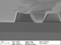
| Profile [o] | 86-87 dg by bghe@nanolab (2015-06-02) |
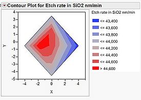
| Wafer uniformity map (click on the image to view a larger image) | |
| SEM profile images | 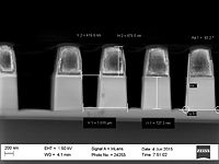 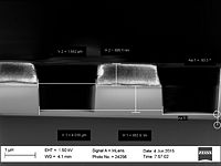 by bghe@nanolab (2015-06-02) |
| Etch rate in barc | |
| Etch rate in KRF resist | 34 nm/min by bghe@nanolab (2015-06-02) |
| Comments |
|
SiO2 etch nLOF
| Parameter | Resist mask |
|---|---|
| Coil Power [W] | 800 |
| Platen Power [W] | 100 |
| Platen temperature [oC] | 0 |
| CF4 flow [sccm] | 30 |
| H2 flow [sccm] | 10 |
| Pressure [mTorr] | 4 |
| Results | Test on wafer with 50% load (Travka 50), by BGHE @nanolab |
|---|---|
| Etch rate of thermal oxide | >110 nm/min (50% etch load) (09-03-2015) |
| Selectivity to resist [:1] | <0.7:1 (SiO2:resist) |
| Wafer uniformity (100mm) | Not known |
| Profile [o] | Not known |
| Wafer uniformity map (click on the image to view a larger image) | Not known |
| SEM profile images | NONE |
| Etch rate in nLOF resist | 1.6µm was removed after 10min |
| Comment | After 10min etch the resist was gone and the etch depth as 1.145µm in the oxide |
SiO2 etch with e-beam resist
| Process flow |
|---|
  px1283lablejan1542014t1  250uc
   at 40mm x y
  pxline400p1000jan142014dt2
  y=    -40    -45   -50   -55mm
  dose   200   240   280   320uc
|
| Parameter | Resist mask |
|---|---|
| Coil Power [W] | 800 |
| Platen Power [W] | 150 |
| Platen temperature [oC] | -10 |
| C4F8 flow [sccm] | 8 |
| H2 flow [sccm] | 30 |
| Pressure [mTorr] | 2.5 |
| Results | Test on 6" wafer, by Peixiong Shi@nanolab |
|---|---|
| Etch rate of thermal oxide | 131 nm/min (15-01-2014) |
| Selectivity to resist [:1] | ~1.8:1 (SiO2:resist) |
| Profile [o] | Not measured |
| Wafer uniformity map (click on the image to view a larger image) | Not known |
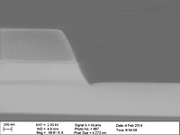
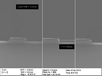
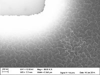
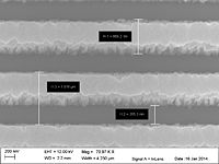
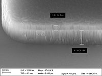
| SEM images |
|

