Specific Process Knowledge/Thin film deposition/Furnace LPCVD TEOS: Difference between revisions
No edit summary |
No edit summary |
||
| (15 intermediate revisions by 4 users not shown) | |||
| Line 1: | Line 1: | ||
'''Feedback to this page''': '''[mailto:thinfilm@ | '''Feedback to this page''': '''[mailto:thinfilm@nanolab.dtu.dk?Subject=Feed%20back%20from%20page%20http://labadviser.nanolab.dtu.dk/index.php/Specific_Process_Knowledge/Thin_film_deposition/Furnace_LPCVD_TEOS) click here]''' | ||
<i> Unless otherwise stated, this page is written by <b>DTU Nanolab internal</b></i> | |||
[[Category: Equipment|Thin film LPCVD TEOS]] | |||
[[Category: Thin Film Deposition|LPCVD TEOS]] | |||
[[Category: Furnaces|LPCVD TEOS]] | |||
==LPCVD (Low Pressure Chemical Vapor Deposition) TEOS== | ==LPCVD (Low Pressure Chemical Vapor Deposition) TEOS== | ||
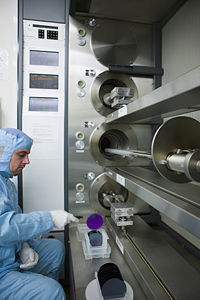
[[Image:160904_danchip_4538.jpg|300x300px|thumb|B3 Furnace LPCVD TEOS. Positioned in cleanroom | [[Image:160904_danchip_4538.jpg|300x300px|thumb|B3 Furnace LPCVD TEOS. Positioned in cleanroom B-1]] | ||
DTU Nanolab has one LPCVD TEOS furnace (installed in 1995). The furnace is a Tempress horizontal furnace. The process is a batch process, where TEOS can be deposited on up to 15 wafer at a time. | |||
TEOS is a silicon dioxide based on tetraethoxysilane. The reactive gas is TEOS, and the deposition takes place at a temperature of 712-720 <sup>o</sup>C (temperature variation over the furnace tube). It is possible to anneal the TEOS layer to improve the electrical properties as well as chemical resistance. The electrical characteristics may also be improved by the addition of O<sub>2</sub> during the deposition process. | |||
TEOS is | The LPCVD TEOS has an excellent step coverage and is very good for trench filling. The film thickness is very uniform over each wafer. | ||
'''The user manual(s), quality control procedure(s) and results, technical information and contact information can be found in LabManager:''' | '''The user manual(s), quality control procedure(s) and results, technical information and contact information can be found in LabManager:''' | ||
'''[http://www.labmanager | '''[http://www.labmanager.dtu.dk/function.php?module=Machine&view=view&mach=85 LPCVD TEOS furnace]''' | ||
'''[https://labmanager.dtu.dk/d4Show.php?id=1926 Furnace computer manual]''' | |||
== Manual for the furnace computer to the A, B, C and E stack furnaces == | |||
The A, B, C and E stack furnaces can be controlled either from a touch screen by each furnace or from a furnace computer. The user manual for the furnace computer can be found here: | |||
[[media:Furnace_computer_manual.pdf|Manual for furnace computers for the A, B, C and E stack furnaces]] | |||
==Process Knowledge== | ==Process Knowledge== | ||
| Line 18: | Line 34: | ||
[[Specific Process Knowledge/Thin film deposition/Deposition of TEOS/Deposition of TEOS using LPCVD|Deposition of TEOS using LPCVD]] | [[Specific Process Knowledge/Thin film deposition/Deposition of TEOS/Deposition of TEOS using LPCVD|Deposition of TEOS using LPCVD]] | ||
==Overview of the performance of the LPCVD TEOS furnace and some process related parameters== | ==Overview of the performance of the LPCVD TEOS furnace and some process related parameters== | ||
| Line 45: | Line 62: | ||
|style="background:LightGrey; color:black"|Process Temperature | |style="background:LightGrey; color:black"|Process Temperature | ||
|style="background:WhiteSmoke; color:black"| | |style="background:WhiteSmoke; color:black"| | ||
* | *712-720 <sup>o</sup>C | ||
|- | |- | ||
|style="background:LightGrey; color:black"|Process pressure | |style="background:LightGrey; color:black"|Process pressure | ||
| Line 54: | Line 71: | ||
|style="background:WhiteSmoke; color:black"| | |style="background:WhiteSmoke; color:black"| | ||
*TEOS: 50 sccm | *TEOS: 50 sccm | ||
*O< | *O<sub>2</sub>: 0 sccm | ||
|- | |- | ||
!style="background:silver; color:black" align="center" valign="center" rowspan="2"|Substrates | !style="background:silver; color:black" align="center" valign="center" rowspan="2"|Substrates | ||
| Line 68: | Line 85: | ||
**from furnaces in stack A or B in cleanroom 2 | **from furnaces in stack A or B in cleanroom 2 | ||
*Quartz wafers (RCA cleaned) | *Quartz wafers (RCA cleaned) | ||
*Silicon carbide sample(RCA cleaned) | |||
|- | |- | ||
|} | |} | ||
== Rules for storage and RCA cleaning of wafers to the B3 furnace == | |||
*[[Specific_Process_Knowledge/Thermal_Process/Storage_and_cleaning_of_wafer_to_the_A,_B,_C_and_E_stack_furnaces|Storage and cleaning of wafer to the B3 furnace]] | |||
Latest revision as of 13:19, 26 June 2023
Feedback to this page: click here
Unless otherwise stated, this page is written by DTU Nanolab internal
LPCVD (Low Pressure Chemical Vapor Deposition) TEOS

DTU Nanolab has one LPCVD TEOS furnace (installed in 1995). The furnace is a Tempress horizontal furnace. The process is a batch process, where TEOS can be deposited on up to 15 wafer at a time.
TEOS is a silicon dioxide based on tetraethoxysilane. The reactive gas is TEOS, and the deposition takes place at a temperature of 712-720 oC (temperature variation over the furnace tube). It is possible to anneal the TEOS layer to improve the electrical properties as well as chemical resistance. The electrical characteristics may also be improved by the addition of O2 during the deposition process.
The LPCVD TEOS has an excellent step coverage and is very good for trench filling. The film thickness is very uniform over each wafer.
The user manual(s), quality control procedure(s) and results, technical information and contact information can be found in LabManager:
Manual for the furnace computer to the A, B, C and E stack furnaces
The A, B, C and E stack furnaces can be controlled either from a touch screen by each furnace or from a furnace computer. The user manual for the furnace computer can be found here:
Manual for furnace computers for the A, B, C and E stack furnaces
Process Knowledge
Please take a look at the process side for deposition of TEOS oxide:
Deposition of TEOS using LPCVD
| Purpose |
Deposition of TEOS - Silicon dioxide based on tetraethoxysilane | |
|---|---|---|
| Performance | Film thickness |
|
| Step coverage |
| |
| Film quality |
| |
| Process parameter range | Process Temperature |
|
| Process pressure |
| |
| Gas flows |
| |
| Substrates | Batch size |
|
| Substrate material allowed |
|
