Specific Process Knowledge/Etch/DRIE-Pegasus/Pegasus-2/Black silicon on Demand: Difference between revisions
No edit summary |
No edit summary |
||
| (21 intermediate revisions by 2 users not shown) | |||
| Line 1: | Line 1: | ||
'''Feedback to this page: | '''Feedback to this page: | ||
[mailto:labadviser@ | [mailto:labadviser@nanolab.dtu.dk?Subject=Feed%20back%20from%20page%20http://labadviser.nanolab.dtu.dk/index.php/Specific_Process_Knowledge/Etch/DRIE-Pegasus/Pegasus-2/Black silicon on Demand click here]''' | ||
<!-- Page reviewed 9/8-2022 jmli --> | |||
{{cc-vthongu1}} | |||
Black silicon (BSi or silicon micro/nano-grass) is a frequently encountered phenomenon in highly directional etching of silicon using mainstream plasma etch tools. Because of the almost perfect light absorption, BSi has found a prominent place in photovoltaic applications. The strongly increased surface area has also shown attractive opportunities in chemical and optical devices. In addition, another already established characteristic of BSi is its ability to prevent cell growth and as such creates anti-bacterial, anti-fogging and self-cleaning surfaces. | Black silicon (BSi or silicon micro/nano-grass) is a frequently encountered phenomenon in highly directional etching of silicon using mainstream plasma etch tools. Because of the almost perfect light absorption, BSi has found a prominent place in photovoltaic applications. The strongly increased surface area has also shown attractive opportunities in chemical and optical devices. In addition, another already established characteristic of BSi is its ability to prevent cell growth and as such creates anti-bacterial, anti-fogging and self-cleaning surfaces. | ||
| Line 16: | Line 19: | ||
Silicon wafers are prepared with 1.5 μm thick resist patterns (AZ MIR 701 DUV resist from MicroChemicals) and exposed using a maskless aligner (MLA150, Heidelberg) to create patterns above 400 nm. Below are some SEM images of BSi nanostructures achieved by the modified CORE process: | Silicon wafers are prepared with 1.5 μm thick resist patterns (AZ MIR 701 DUV resist from MicroChemicals) and exposed using a maskless aligner (MLA150, Heidelberg) to create patterns above 400 nm. Below are some SEM images of BSi nanostructures achieved by the modified CORE process: | ||
<gallery caption="" widths=" | <gallery caption="" widths="360px" heights="280px" perrow="2"> | ||
File:BSi free.png|''''' 1 µm silicon pillars etched with a BSi-free recipe''''' | File:BSi free.png|''''' 1 µm silicon pillars etched with a BSi-free recipe''''' | ||
File:BSi full.png|''''' 1 µm silicon pillars etched first with a BSi-free recipe and then continued with a BSi-full recipe''''' | File:BSi full.png|''''' 1 µm silicon pillars etched first with a BSi-free recipe and then continued with a BSi-full recipe''''' | ||
</gallery> | </gallery> | ||
[[File:PR strip.png|800px|left|thumb|''''' By removing the mask on top of the pillars, the BSi can be formed on top of the these pillars''''']] | [[File:PR strip.png|800px|left|thumb|''''' By removing the mask on top of the pillars, the BSi can be formed on top of the these pillars''''']] | ||
Revision as of 16:35, 1 May 2023
Feedback to this page: silicon on Demand click here
Black silicon (BSi or silicon micro/nano-grass) is a frequently encountered phenomenon in highly directional etching of silicon using mainstream plasma etch tools. Because of the almost perfect light absorption, BSi has found a prominent place in photovoltaic applications. The strongly increased surface area has also shown attractive opportunities in chemical and optical devices. In addition, another already established characteristic of BSi is its ability to prevent cell growth and as such creates anti-bacterial, anti-fogging and self-cleaning surfaces.
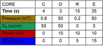
By manipulating process parameters and utilizing the self-limiting property of the oxidation step, the CORE process can easily be modified to create either BSi-full or BSi-free surfaces independent of the aspect ratio of the etching features. Therefore this method provides a versatile tool for creating BSi anywhere at anytime or - as we call it - ‘BSi on Demand’.
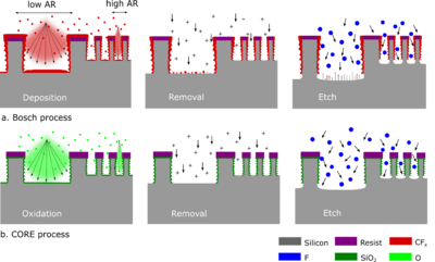
On DRIE-Pegasus 2, the formation and controllabilty of BSi in the CORE sequence is different from how BSi presents itself in the FC-based sequences. The schematic illustration of BSi formation in the Bosch process and BSi-free in the CORE sequence is shown below.
Example of the CORE recipe for BSi
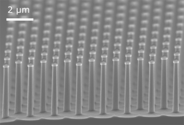
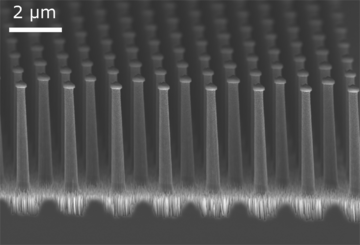
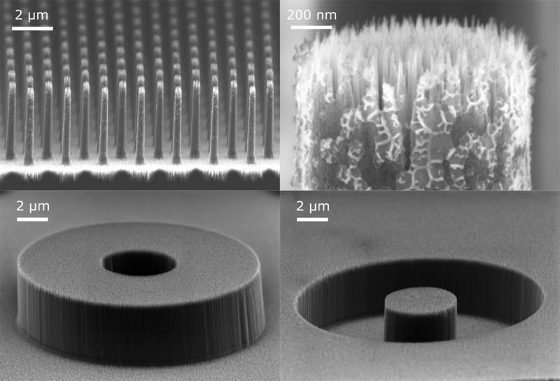
Silicon wafers are prepared with 1.5 μm thick resist patterns (AZ MIR 701 DUV resist from MicroChemicals) and exposed using a maskless aligner (MLA150, Heidelberg) to create patterns above 400 nm. Below are some SEM images of BSi nanostructures achieved by the modified CORE process:
-
1 µm silicon pillars etched with a BSi-free recipe
-
1 µm silicon pillars etched first with a BSi-free recipe and then continued with a BSi-full recipe
For more details, please contact Henri Jansen (henrija@dtu.dk) or Vy Thi Hoang Nguyen (vthongu@dtu.dk).

