Specific Process Knowledge/Etch/IBE⁄IBSD Ionfab 300/IBE Ti etch: Difference between revisions
Appearance
No edit summary |
No edit summary |
||
| (5 intermediate revisions by 2 users not shown) | |||
| Line 1: | Line 1: | ||
'''Feedback to this page''': '''[mailto:labadviser@nanolab.dtu.dk?Subject=Feed%20back%20from%20page%20http://labadviser.nanolab.dtu.dk/index.php/Specific_Process_Knowledge/Etch/IBE⁄IBSD_Ionfab_300/IBE_Ti_etch click here]''' | |||
<br> {{CC-bghe1}} | |||
==Results from the acceptance test in February 2011== | ==Results from the acceptance test in February 2011== | ||
'''Acceptance test for Ti etch:''' | '''Acceptance test for Ti etch :''' | ||
{| border="2" cellspacing="0" cellpadding="2" | {| border="2" cellspacing="0" cellpadding="2" | ||
|- | |- | ||
| Line 12: | Line 15: | ||
*50 mm SSP Si wafer | *50 mm SSP Si wafer | ||
*525 µm thick | *525 µm thick | ||
*Supplied by | *Supplied by Nanolab | ||
|. | |. | ||
|- | |- | ||
| Line 29: | Line 32: | ||
!style="background:silver; color:black" align="left" valign="top"|Features to be etched | !style="background:silver; color:black" align="left" valign="top"|Features to be etched | ||
|style="background:WhiteSmoke; color:black"| | |style="background:WhiteSmoke; color:black"| | ||
* | *300 nm - 3µm dots and lines + a square of 200µmx200µm | ||
|. | |. | ||
|- | |- | ||
| Line 40: | Line 43: | ||
!style="background:silver; color:black" align="left" valign="top"|Etch rate | !style="background:silver; color:black" align="left" valign="top"|Etch rate | ||
|style="background:WhiteSmoke; color:black"| | |style="background:WhiteSmoke; color:black"| | ||
*> | *>80 nm/min | ||
| | | | ||
* | *22 nm/min +- 0.3nm/min (one standard deviation) | ||
|- | |- | ||
!style="background:silver; color:black" align="left" valign="top"|Etch rate uniformity | !style="background:silver; color:black" align="left" valign="top"|Etch rate uniformity | ||
| Line 56: | Line 59: | ||
*+-(0.8% +-0.5%) | *+-(0.8% +-0.5%) | ||
|- | |- | ||
!style="background:silver; color:black" align="left" valign="top"|Selectivity ( | !style="background:silver; color:black" align="left" valign="top"|Selectivity (Ti etch rate/ZEP etch rate) | ||
|style="background:WhiteSmoke; color:black"| | |style="background:WhiteSmoke; color:black"| | ||
*At least 1:1 | *At least 1:1 | ||
| Line 75: | Line 78: | ||
!Ti etch acceptance | !Ti etch acceptance | ||
|- | |- | ||
| | |Neutralizer current [mA] | ||
|550 | |550 | ||
|- | |- | ||
Revision as of 15:45, 6 February 2023
Feedback to this page: click here
The content on this page, including all images and pictures, was created by Berit Herstrøm @ DTU Nanolab (BGHE), unless otherwise stated.
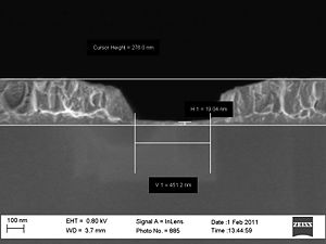
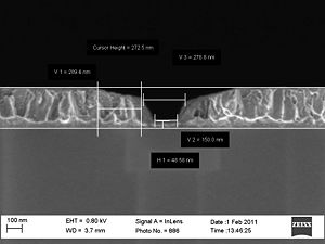
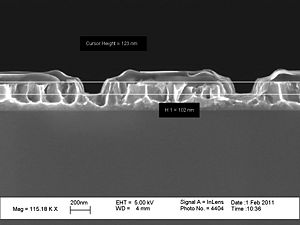
Results from the acceptance test in February 2011
Acceptance test for Ti etch :
| . | Acceptance Criteria |
Acceptance Results |
|---|---|---|
| Substrate information |
|
. |
| Material to be etched |
|
. |
| Mask information |
|
. |
| Features to be etched |
|
. |
| Etch depth |
|
|
| Etch rate |
|
|
| Etch rate uniformity |
|
|
| Reproducibility |
|
|
| Selectivity (Ti etch rate/ZEP etch rate) |
|
|
| Etch profile |
|
|
Process parameters for the acceptance test
| Parameter | Ti etch acceptance |
|---|---|
| Neutralizer current [mA] | 550 |
| RF Power [W] | 1200 |
| Beam current [mA] | 500 |
| Beam voltage [V] | 600 |
| Beam accelerator voltage | 400 |
| Ar flow to neutralizer [sccm] | 6.0 |
| Ar flow to beam [sccm] | 6.0 |
| Rotation speed [rpm] | 20 |
| Stage angle [degrees] | 20 |


