Specific Process Knowledge/Etch/IBE⁄IBSD Ionfab 300/IBE Au etch: Difference between revisions
Appearance
No edit summary |
|||
| (28 intermediate revisions by 2 users not shown) | |||
| Line 1: | Line 1: | ||
'''Feedback to this page''': '''[mailto:labadviser@nanolab.dtu.dk?Subject=Feed%20back%20from%20page%20http://labadviser.nanolab.dtu.dk/index.php/Specific_Process_Knowledge/Etch/IBE⁄IBSD_Ionfab_300/IBE_Au_etch click here]''' | |||
<br> {{CC-bghe1}} | |||
==Results from the acceptance test in February 2011== | ==Results from the acceptance test in February 2011== | ||
'''Acceptance test for Au etch:''' | '''Acceptance test for Au etch:''' | ||
| Line 12: | Line 16: | ||
*50 mm SSP Si wafer | *50 mm SSP Si wafer | ||
*525 µm thick | *525 µm thick | ||
*Supplied by | *Supplied by Nanolab | ||
|. | |. | ||
|- | |- | ||
| Line 23: | Line 27: | ||
|style="background:WhiteSmoke; color:black"| | |style="background:WhiteSmoke; color:black"| | ||
*E-beam resist mask: | *E-beam resist mask: | ||
# | # 400 nm of spin coated ZEP520A e-beam resist | ||
#Patterned by E-beam lithography | #Patterned by E-beam lithography | ||
|. | |. | ||
| Line 29: | Line 33: | ||
!style="background:silver; color:black" align="left" valign="top"|Features to be etched | !style="background:silver; color:black" align="left" valign="top"|Features to be etched | ||
|style="background:WhiteSmoke; color:black"| | |style="background:WhiteSmoke; color:black"| | ||
* | *300 nm - 3µm dots and lines + a square of 200µmx200µm | ||
|. | |. | ||
|- | |- | ||
| Line 64: | Line 68: | ||
!style="background:silver; color:black" align="left" valign="top"|Etch profile | !style="background:silver; color:black" align="left" valign="top"|Etch profile | ||
|style="background:WhiteSmoke; color:black"| | |style="background:WhiteSmoke; color:black"| | ||
*70- | *70-90 dg. | ||
| | | | ||
* | *75 dg | ||
|} | |} | ||
| Line 74: | Line 78: | ||
!Au etch acceptance | !Au etch acceptance | ||
|- | |- | ||
| | |Neutralizer current [mA] | ||
|550 | |550 | ||
|- | |- | ||
| Line 108: | Line 112: | ||
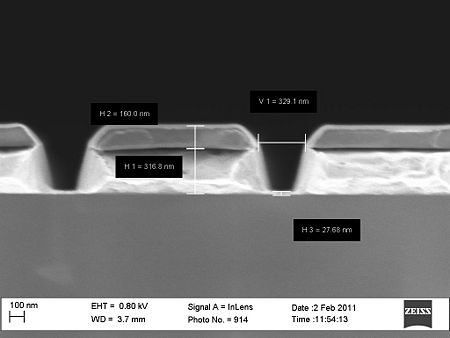
===Some SEM profile images of the etched Au=== | ===Some SEM profile images of the etched Au=== | ||
{| border="1" cellspacing="1" cellpadding="2" | {| border="1" cellspacing="1" cellpadding="2" | ||
| | |||
[[image:IBE accpetance S18-AU-ZEP3.jpg|450x450px|thumb|center|s18-Au-ZEP3]] | [[image:IBE accpetance S18-AU-ZEP3.jpg|450x450px|thumb|center|s18-Au-ZEP3]] | ||
| | |||
[[image:IBE acceptance S18-AU-ZEP5.jpg|450x450px|thumb|center|s18-Au-ZEP5]] | [[image:IBE acceptance S18-AU-ZEP5.jpg|450x450px|thumb|center|s18-Au-ZEP5]] | ||
|} | |} | ||
==IBE Au etch with Ti mask== | |||
''by bghe@nanolab'' | |||
Work has been started to find a good process for etching gold with a Titanium mask with high selectivity. | |||
Work has been started to find a good process for etching gold with a Titanium mask with high | |||
{|border="1" cellspacing="1" cellpadding="3" style="text-align:left;" | {|border="1" cellspacing="1" cellpadding="3" style="text-align:left;" | ||
| Line 135: | Line 135: | ||
|- | |- | ||
|-style="background:WhiteSmoke; color:black" | |-style="background:WhiteSmoke; color:black" | ||
! | !General description | ||
|This recipe has a good selectivity between ZEP520A resist and Ti, which makes it good for | |This recipe has a good selectivity between ZEP520A resist and Ti, which makes it good for patterning the Ti that should be used as masking layer for the Au etch. It can also be used to etch Au if the selectivity to the mask is good enough. | ||
|This recipe has especially good selectivity between Ti and Au which makes it good for gold etching using a thin Ti mask as masking layer. The selectivity to resist is very bad so do not use it with a resist mask. | |This recipe has especially good selectivity between Ti and Au which makes it good for gold etching using a thin Ti mask as masking layer. The selectivity to resist is very bad so do not use it with a resist mask. | ||
|- | |- | ||
| Line 144: | Line 144: | ||
!Recipe name | !Recipe name | ||
| | | | ||
Ti acceptance 20111129 | |||
| | | | ||
Au_acceptance_with_O2 | Au_acceptance_with_O2 | ||
| Line 186: | Line 186: | ||
!Etch rate in resist | !Etch rate in resist | ||
| | | | ||
12. | 12.8 nm/min (15-12-2011) | ||
| | | | ||
72 nm/min (13-12-2011) | |||
|- | |- | ||
| Line 218: | Line 218: | ||
!Selectivity Au/Ti | !Selectivity Au/Ti | ||
| | | | ||
3. | 3.9 (15-12-2011) | ||
| | | | ||
9. | 9.9 (13-12-2011) | ||
|-valign="top" | |||
!SEM images of the etch profile (click to view a larger image) | |||
| | |||
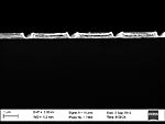
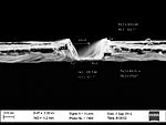
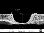
<gallery caption="600nm lines etched for 14 min (15-12-2011)" widths="150px" heights="150px" perrow="2"> | |||
image:IBE_Au_Ti_nr13_1.jpg|Several line profiles through Ti and Au. | |||
image:IBE_Au_Ti_nr13_2.jpg|Line profile through Ti and Au. | |||
</gallery> | |||
<gallery widths="150px" height ="150px" perrow="3"> | |||
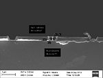
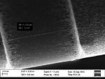
image:IBE_Au_Ti_uden_Ti_nr13_1.jpg|Several line profiles in Au after Ti has been removed. | |||
image:IBE_Au_Ti_uden_Ti_nr13_2.jpg|Line profile in Au after Ti has been removed. | |||
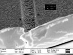
image:IBE_Au_Ti_uden_Ti_nr13_3.jpg|Line in Au after Ti has been removed. Sample is tilted | |||
</gallery> | |||
| | |||
<gallery caption="Ti mask etched for 6min30sec with recipe ''test Ti acceptance 20111129''. The Au was etched for 7min with recipe ''Au_acceptance_with_O2''. The result was less fenching because a thinner mask was used (Ti instead off resist)" widths="150px" height="150px" perrow="3" > | |||
image:IBE_Au_Ti_w14_20130926_500nmT_BHF5min_2.jpg|Tilted line in Au after Ti has been removed. | |||
image:IBE_Au_Ti_W14_20130926_500nm_1.jpg|Profile in Au after Ti has been removed. | |||
image:IBE_Au_Ti_W14_20130926_3000nmT_5.jpg|Tilted line in Au after Ti has been removed. | |||
</gallery> | |||
|- | |- | ||
|} | |} | ||
<br clear="all" /> | <br clear="all" /> | ||
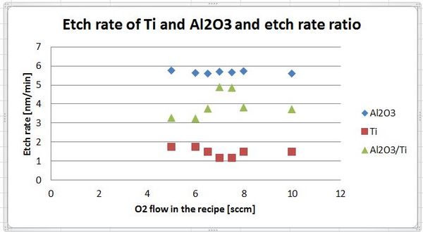
==Al2O3 using Ti mask etching with the "Au acceptance recipe"== | |||
''This work was done by Sezer Köse @fotonik April 2019'' <br> | |||
[[File:Sezer Al2O3 and Ti.JPG|600px]] | |||
Revision as of 15:25, 6 February 2023
Feedback to this page: click here
The content on this page, including all images and pictures, was created by Berit Herstrøm @ DTU Nanolab (BGHE), unless otherwise stated.
Results from the acceptance test in February 2011
Acceptance test for Au etch:
| . | Acceptance Criteria |
Acceptance Results |
|---|---|---|
| Substrate information |
|
. |
| Material to be etched |
|
. |
| Mask information |
|
. |
| Features to be etched |
|
. |
| Etch depth |
|
|
| Etch rate |
|
|
| Etch rate uniformity |
|
|
| Reproducibility |
|
|
| Selectivity (Au etch rate/ZEP etch rate) |
|
|
| Etch profile |
|
|
Process parameters for the acceptance test
| Parameter | Au etch acceptance |
|---|---|
| Neutralizer current [mA] | 550 |
| RF Power [W] | 1300 |
| Beam current [mA] | 500 |
| Beam voltage [V] | 600 |
| Beam accelerator voltage | 400 |
| Ar flow to neutralizer [sccm] | 5.0 |
| Ar flow to beam [sccm] | 10.0 |
| Rotation speed [rpm] | 20 |
| Stage angle [degrees] | 30 |
Some SEM profile images of the etched Au
 |
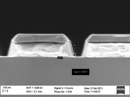 |
IBE Au etch with Ti mask
by bghe@nanolab
Work has been started to find a good process for etching gold with a Titanium mask with high selectivity.
| Ti etch test with Zep520A as mask - To etch the Ti mask | Au etch test with high selectivity to Ti | |
|---|---|---|
| General description | This recipe has a good selectivity between ZEP520A resist and Ti, which makes it good for patterning the Ti that should be used as masking layer for the Au etch. It can also be used to etch Au if the selectivity to the mask is good enough. | This recipe has especially good selectivity between Ti and Au which makes it good for gold etching using a thin Ti mask as masking layer. The selectivity to resist is very bad so do not use it with a resist mask. |
| Recipe name |
Ti acceptance 20111129 |
Au_acceptance_with_O2 |
| IBE parameters |
|
|
| Results | ||
| Etch rate in resist |
12.8 nm/min (15-12-2011) |
72 nm/min (13-12-2011) |
| Etch rate in Au |
32.7nm/min (15-12-2011) |
42.6nm/min (13-12-2011) |
| Etch rate in Ti |
8.3nm/min (15-12-2011) |
4.3nm/min (13-12-2011) |
| Selectivity Ti/Zep |
0.65 (15-12-2011) |
0.06 (13-12-2011) |
| Selectivity Au/Ti |
3.9 (15-12-2011) |
9.9 (13-12-2011) |
| SEM images of the etch profile (click to view a larger image) |
|
|

