Specific Process Knowledge/Lithography/mrEBL6000: Difference between revisions
mNo edit summary |
|||
| (13 intermediate revisions by 2 users not shown) | |||
| Line 1: | Line 1: | ||
<br> | |||
mrEBL6000 works as a negative e-beam resist but is also UV sensitive, why resist and coated wafers should be kept in yellow rooms only. When carrying the wafers to the e-beam writer, use a black or blue box for protection. While mounting the wafers in the e-beam cassettes, you can turn off the white light in the e-beam room and turn on the yellow light which is located above the pre-aligner setup. Please mount as close to exposure as possible and turn of the with light outside the room and place a note on the door not to turn on light while the cassette is in the stocker. | |||
mrEBL6000 is a chemically amplified resist, i.e. immediately after e-beam exposure, the wafers require a post-exposure bake. If no post-exposure bake is performed, the resist is not crosslinked and will most likely dissolve during development. | |||
This resist can be used as standard negative resist at Nanolab, but due to limited use, we often need to buy a new bottle, hence please ask long time (up to 3 months) in advance for this chemical. or by it yourself! | |||
<br> | <br> | ||
<br> | <br> | ||
<br> | <br> | ||
== 3 week project on mrEBL6000 by William Tiddi == | == 3 week project on mrEBL6000 by William Tiddi == | ||
| Line 173: | Line 152: | ||
==Contrast Curve== | ==Contrast Curve== | ||
The contrast curve is measured on lines 100 nm in width, exposed with doses in the range of 6-63 µC/cm2. After exposure, the sample has been post-exposure baked 5 min @ 110 degree C. Development is performed with mr-DEV 600 in 40s followed by an IPA rinse 60s. | |||
These measurements are performed by WILTID April 2015. | |||
[[File:mrEBL_contrast.png|right|500px]] | |||
<br> | |||
<br> | |||
[[File: | [[File:mrEBL_doses6_33.png|left|600px]] | ||
<br> | <br> | ||
<br> | <br> | ||
Latest revision as of 12:17, 20 August 2021
mrEBL6000 works as a negative e-beam resist but is also UV sensitive, why resist and coated wafers should be kept in yellow rooms only. When carrying the wafers to the e-beam writer, use a black or blue box for protection. While mounting the wafers in the e-beam cassettes, you can turn off the white light in the e-beam room and turn on the yellow light which is located above the pre-aligner setup. Please mount as close to exposure as possible and turn of the with light outside the room and place a note on the door not to turn on light while the cassette is in the stocker.
mrEBL6000 is a chemically amplified resist, i.e. immediately after e-beam exposure, the wafers require a post-exposure bake. If no post-exposure bake is performed, the resist is not crosslinked and will most likely dissolve during development.
This resist can be used as standard negative resist at Nanolab, but due to limited use, we often need to buy a new bottle, hence please ask long time (up to 3 months) in advance for this chemical. or by it yourself!
3 week project on mrEBL6000 by William Tiddi
mrEBL6000 was studied April 2015 by William Tiddi; the report can be found here.
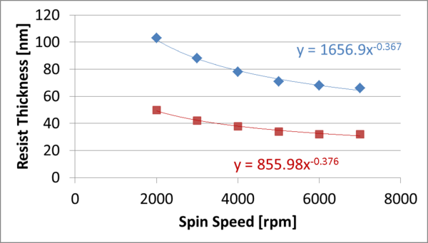
Spin Curve

The thickness is measured on VASE Ellipsometer using a simple Cauchy model for a transparent polymer on Si. The measurements are performed at one incidence angle (70 degrees) only.
9 points on each 4" wafer has been measured; the standard deviation thus representing the homogeinity of the film on the 4" wafers.
| MicroResist mr EBL 6000. Spin coated on Spin Coater: Manual LabSpin A-5, WILTID, 2015. Softbake 3 min @ 110 degC. | ||
|---|---|---|
| Spin Speed [rpm] | Thickness [nm] | St Dev |
| 2000 | 103 | 0.5 |
| 3000 | 88 | 0.4 |
| 4000 | 78 | 0.4 |
| 5000 | 71 | 0.7 |
| 6000 | 68 | 0.5 |
| 7000 | 66 | 0.6 |
| MicroResist mr EBL 6000 diluted 1:1 in anisole. Spin coated on Spin Coater: Manual LabSpin A-5, WILTID, 2015. Softbake 3 min @ 110 degC. | ||
|---|---|---|
| Spin Speed [rpm] | Thickness [nm] | St Dev |
| 2000 | 50 | 0.2 |
| 3000 | 42 | 0.5 |
| 4000 | 38 | 0.5 |
| 5000 | 34 | 0.3 |
| 6000 | 32 | 0.3 |
| 7000 | 32 | 0.3 |
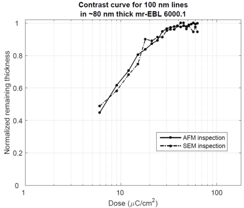
Contrast Curve
The contrast curve is measured on lines 100 nm in width, exposed with doses in the range of 6-63 µC/cm2. After exposure, the sample has been post-exposure baked 5 min @ 110 degree C. Development is performed with mr-DEV 600 in 40s followed by an IPA rinse 60s. These measurements are performed by WILTID April 2015.


