LabAdviser/Technology Research/Fabrication of Hyperbolic Metamaterials using Atomic Layer Deposition/TIO ALU Gratings Procces flow: Difference between revisions
| Line 56: | Line 56: | ||
|To ensure that remainings of DUV resist are gone, samples are treated by O<sub>2</sub>/N<sub>2</sub> plasma. (Optional step) | |To ensure that remainings of DUV resist are gone, samples are treated by O<sub>2</sub>/N<sub>2</sub> plasma. (Optional step) | ||
|[[Specific_Process_Knowledge/Lithography/Strip#Plasma_Asher_2| Plasma Asher 2]]. | |[[Specific_Process_Knowledge/Lithography/Strip#Plasma_Asher_2| Plasma Asher 2]]. | ||
|[[image | |[[no image]] | ||
|- | |- | ||
Revision as of 17:39, 31 May 2016
Procces flow description
The substrates for the samples were fabricated by depositing 1 μm of Si3N4 (the resonator layer) on 100 mm silicon < 100 > wafers using low-pressure chemical vapor deposition. The process was carried out at 780C with ammonia (NH3) and dichlorosilane (SiH2Cl2) as reactive gases. Thickness and refractive index of the deposited silicon nitride was measured and confirmed using spectroscopic ellipsometry. The deposited Si3N4 film was carefully analyzed for existence of cracks, particles and other defects using dark field optical microscopy. The best-quality wafer with Si3N4 was selected and cleaved in pieces, which were used as substrates for the deposition of Al2O3/TiO2 multilayers. Before inserting each substrate into the ALD reactor, it was placed on a Si carrier wafer. Therefore the Al2O3/TiO2 multilayers were grown not only on the Si3N4 layer but also on the dummy carrier wafer. After the ALD process was completed, the dummy was cleaved and its cross-section was characterized using scanning electron microscopy (SEM). The SEM images reveal high-quality homogeneous, conformal coatings, as seen in the examples in Figs 1. Such a method of deposited multilayers characterization turned out to be more feasible than the direct SEM characterization of multilayers on Si3N4, since the latter suffers from issues related to charge accumulation on the silicon nitride.
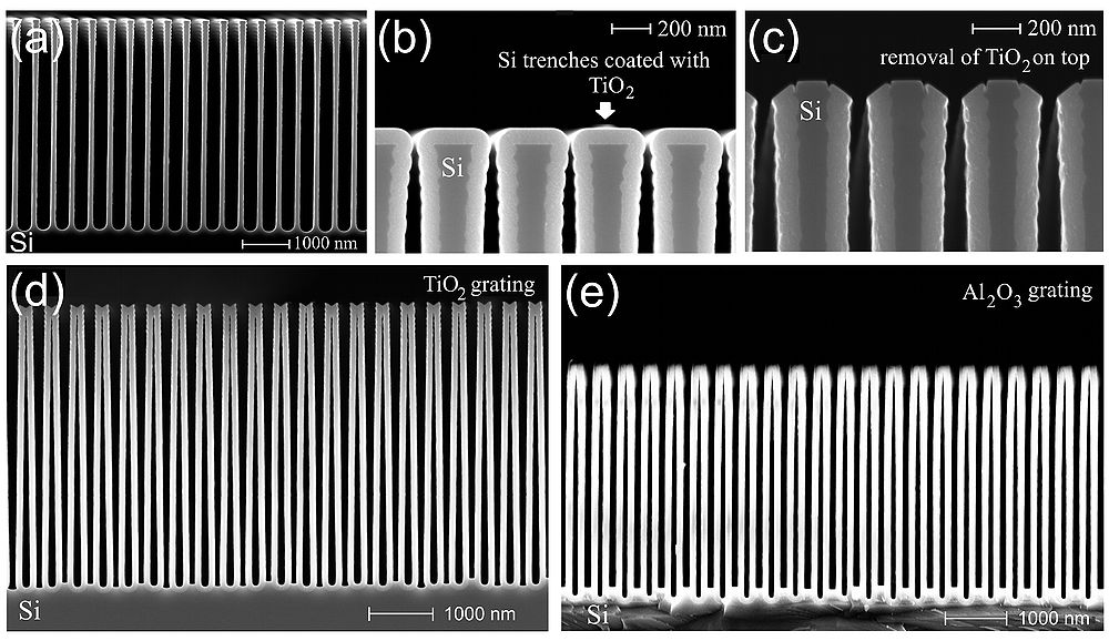
High aspect ratio Al2O3 and TiO2 nanogratings.

Process flow
Hej Evgeniy
Jeg har lagt dette eksemple på et process flow ind. Alt tekst og billeder skal selvfølgelig erstattes af relevante process steps for denne artikel.
Mvh. Berit
| Step | Description | LabAdviser link | Image showing the step | |
|---|---|---|---|---|
| 2.1 | Plasma surface treatment | To ensure clean surface, the 100 mm Si wafer is treated by O2/N2 plasma. (Optional step) | Plasma Asher 2 | |
| 2.2 | DUV Resist patterning | DUV | DUV Stepper Lithography. | |
| 2.3 | Deep reactive ion etching (DRIE) | DRIE | DRIE Pegasus. | |
| 2.4 | Plasma surface treatment | To ensure that remainings of DUV resist are gone, samples are treated by O2/N2 plasma. (Optional step) | Plasma Asher 2. | no image |
| 2.5 | Scanning Electron Microscopy inspection | By cleaving the sample it is possible to inspect DRIE etched Si strenches in cross-sectional mode | SEM Supra 2 |  |
| 2.6 | XPS inspection for elemental trace analysis | XPS can be used in depth profile mode. Ar+ ions erodes the surface of multilayers, allowing the inspection of each layer. | Equipment used: XPS-ThermoScientific. Results of depth profiling presented: XPS results . |  |
_nanogratings.JPG)
_nanogratings.JPG)
_nanogratings.JPG)